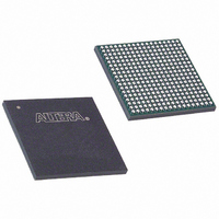
EP1C4F324C8 Altera, EP1C4F324C8 Datasheet - Page 63

EP1C4F324C8
Manufacturer Part Number
EP1C4F324C8
Description
IC CYCLONE FPGA 4K LE 324-FBGA
Manufacturer
Altera
Series
Cyclone®r
Datasheet
1.EP1C3T144C8.pdf
(106 pages)
Specifications of EP1C4F324C8
Number Of Logic Elements/cells
4000
Number Of Labs/clbs
400
Total Ram Bits
78336
Number Of I /o
249
Voltage - Supply
1.425 V ~ 1.575 V
Mounting Type
Surface Mount
Operating Temperature
0°C ~ 85°C
Package / Case
324-FBGA
Lead Free Status / RoHS Status
Contains lead / RoHS non-compliant
Number Of Gates
-
Other names
544-1044
Available stocks
Company
Part Number
Manufacturer
Quantity
Price
Company:
Part Number:
EP1C4F324C8
Manufacturer:
ALTERA
Quantity:
591
Part Number:
EP1C4F324C8
Manufacturer:
ALTERA/阿尔特拉
Quantity:
20 000
Company:
Part Number:
EP1C4F324C8N
Manufacturer:
ALTERA
Quantity:
648
Part Number:
EP1C4F324C8N
Manufacturer:
ALTERA
Quantity:
20 000
IEEE Std. 1149.1
(JTAG) Boundary
Scan Support
Altera Corporation
May 2008
SAMPLE
EXTEST
BYPASS
C51003-1.4
Table 3–1. Cyclone JTAG Instructions (Part 1 of 2)
JTAG Instruction
/
PRELOAD
(1)
00 0000 0101
00 0000 0000
11 1111 1111
Instruction Code
All Cyclone
IEEE Std. 1149.1a-1990 specification. JTAG boundary-scan testing can be
performed either before or after, but not during configuration. Cyclone
devices can also use the JTAG port for configuration together with either
the Quartus
Byte-Code Files (.jbc).
Cyclone devices support reconfiguring the I/O standard settings on the
IOE through the JTAG BST chain. The JTAG chain can update the I/O
standard for all input and output pins any time before or during user
mode. Designers can use this ability for JTAG testing before configuration
when some of the Cyclone pins drive or receive from other devices on the
board using voltage-referenced standards. Since the Cyclone device
might not be configured before JTAG testing, the I/O pins might not be
configured for appropriate electrical standards for chip-to-chip
communication. Programming those I/O standards via JTAG allows
designers to fully test I/O connection to other devices.
The JTAG pins support 1.5-V/1.8-V or 2.5-V/3.3-V I/O standards. The
TDO pin voltage is determined by the V
The bank V
3.3-V compatible.
Cyclone devices also use the JTAG port to monitor the operation of the
device with the SignalTap
support the JTAG instructions shown in
CCIO
®
®
Allows a snapshot of signals at the device pins to be captured and
examined during normal device operation, and permits an initial
data pattern to be output at the device pins. Also used by the
SignalTap II embedded logic analyzer.
Allows the external circuitry and board-level interconnects to be
tested by forcing a test pattern at the output pins and capturing test
results at the input pins.
Places the 1-bit bypass register between the TDI and TDO pins,
which allows the BST data to pass synchronously through selected
devices to adjacent devices during normal device operation.
devices provide JTAG BST circuitry that complies with the
II software or hardware using either Jam Files (.jam) or Jam
selects whether the JTAG inputs are 1.5-V, 1.8-V, 2.5-V, or
3. Configuration and Testing
®
II embedded logic analyzer. Cyclone devices
Description
CCIO
Table
of the bank where it resides.
3–1.
Preliminary
3–1


