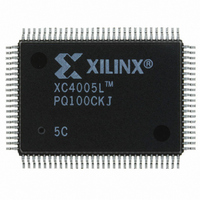
XC4005L-5PQ100C Xilinx Inc, XC4005L-5PQ100C Datasheet - Page 24

XC4005L-5PQ100C
Manufacturer Part Number
XC4005L-5PQ100C
Description
IC 3.3V FPGA 196 CLB'S 100-PQFP
Manufacturer
Xilinx Inc
Series
XC4000r
Datasheet
1.XC4005L-5PC84C.pdf
(175 pages)
Specifications of XC4005L-5PQ100C
Number Of Logic Elements/cells
466
Number Of Labs/clbs
196
Total Ram Bits
6272
Number Of I /o
77
Number Of Gates
5000
Voltage - Supply
3 V ~ 3.6 V
Mounting Type
Surface Mount
Operating Temperature
0°C ~ 85°C
Package / Case
100-BQFP
Lead Free Status / RoHS Status
Contains lead / RoHS non-compliant
Other names
122-1121
Available stocks
Company
Part Number
Manufacturer
Quantity
Price
XC4000 Series Field Programmable Gate Arrays
An output can be configured as open-drain (open-collector)
by placing an OBUFT symbol in a schematic or HDL code,
then tying the 3-state pin (T) to the output signal, and the
input pin (I) to Ground. (See
Output Slew Rate
The slew rate of each output buffer is, by default, reduced,
to minimize power bus transients when switching non-criti-
cal signals. For critical signals, attach a FAST attribute or
property to the output buffer or flip-flop.
For XC4000E devices, maximum total capacitive load for
simultaneous fast mode switching in the same direction is
200 pF for all package pins between each Power/Ground
pin pair. For XC4000EX devices, additional internal Power/
Ground pin pairs are connected to special Power and
Ground planes within the packages, to reduce ground
bounce. Therefore, the maximum total capacitive load is
300 pF between each external Power/Ground pin pair.
Maximum loading may vary for the low-voltage devices.
For slew-rate limited outputs this total is two times larger for
each device type: 400 pF for XC4000E devices and 600 pF
for XC4000EX devices. This maximum capacitive load
should not be exceeded, as it can result in ground bounce
of greater than 1.5 V amplitude and more than 5 ns dura-
tion. This level of ground bounce may cause undesired
transient behavior on an output, or in the internal logic.
This restriction is common to all high-speed digital ICs, and
is not particular to Xilinx or the XC4000 Series.
XC4000-Series devices have a feature called “Soft Start-
up,” designed to reduce ground bounce when all outputs
are turned on simultaneously at the end of configuration.
When the configuration process is finished and the device
starts up, the first activation of the outputs is automatically
slew-rate limited. Immediately following the initial activation
of the I/O, the slew rate of the individual outputs is deter-
mined by the individual configuration option for each IOB.
Global Three-State
A separate Global 3-State line (not shown in
Figure
state, unless boundary scan is enabled and is executing an
EXTEST instruction. This global net (GTS) does not com-
pete with other routing resources; it uses a dedicated distri-
bution network.
4-28
Figure 19: Open-Drain Output
17) forces all FPGA outputs to the high-impedance
OBUFT
Figure
OPAD
X6702
19.)
Figure 16
or
GTS can be driven from any user-programmable pin as a
global 3-state input. To use this global net, place an input
pad and input buffer in the schematic or HDL code, driving
the GTS pin of the STARTUP symbol. A specific pin loca-
tion can be assigned to this input using a LOC attribute or
property, just as with any other user-programmable pad.
An inverter can optionally be inserted after the input buffer
to invert the sense of the Global 3-State signal. Using GTS
is similar to GSR. See
Alternatively, GTS can be driven from any internal node.
Output Multiplexer/2-Input Function Generator
(XC4000EX only)
As shown in
XC4000EX IOB contains an additional multiplexer not avail-
able in the XC4000E IOB. The multiplexer can also be con-
figured as a 2-input function generator, implementing a
pass-gate, AND-gate, OR-gate, or XOR-gate, with 0, 1, or 2
inverted inputs. The logic used to implement these func-
tions is shown in the upper gray area of
When configured as a multiplexer, this feature allows two
output signals to time-share the same output pad; effec-
tively doubling the number of device outputs without requir-
ing a larger, more expensive package.
When the MUX is configured as a 2-input function genera-
tor, logic can be implemented within the IOB itself. Com-
bined with either a FastCLK or Global Early buffer, this
arrangement allows very high-speed gating of a single sig-
nal. For example, a wide decoder can be implemented in
CLBs, and its output gated with a Read or Write Strobe
driven by a FastCLK buffer, as shown in
critical-path pin-to-pin delay of this circuit is less than 6
nanoseconds.
XC4000XL devices.)
As shown in
Clock, and Clock Enable have different delays and different
flexibilities regarding polarity. Additionally, Output Clock
sources are more limited than the other inputs. Therefore,
the Xilinx software does not move logic into the IOB func-
tion generators unless explicitly directed to do so.
Figure 20: Fast Pin-to-Pin Path in XC4000E
IPAD
from
internal
logic
Figure 17 on page
Figure
BUFFCLK
(This value may not be achievable in
17, the IOB input pins Out, Output
Figure 2 on page 13
September 18, 1996 (Version 1.04)
OAND2
25, the output path in the
F
Figure
Figure
for details.
17.
OPAD
FAST
X6698
20. The


