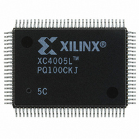
XC4005L-5PQ100C Xilinx Inc, XC4005L-5PQ100C Datasheet - Page 44

XC4005L-5PQ100C
Manufacturer Part Number
XC4005L-5PQ100C
Description
IC 3.3V FPGA 196 CLB'S 100-PQFP
Manufacturer
Xilinx Inc
Series
XC4000r
Datasheet
1.XC4005L-5PC84C.pdf
(175 pages)
Specifications of XC4005L-5PQ100C
Number Of Logic Elements/cells
466
Number Of Labs/clbs
196
Total Ram Bits
6272
Number Of I /o
77
Number Of Gates
5000
Voltage - Supply
3 V ~ 3.6 V
Mounting Type
Surface Mount
Operating Temperature
0°C ~ 85°C
Package / Case
100-BQFP
Lead Free Status / RoHS Status
Contains lead / RoHS non-compliant
Other names
122-1121
Available stocks
Company
Part Number
Manufacturer
Quantity
Price
XC4000 Series Field Programmable Gate Arrays
Table 18: Pin Descriptions (Continued)
4-48
(XC4000EX
(XC4000EX
(XC4000E
(XC4000E
Pin Name
TDI, TCK,
PGCK1 -
SGCK1 -
FCLK1 -
PGCK4
SGCK4
GCK1 -
FCLK4
GCK8
HDC
only)
only)
only)
only)
TDO
TMS
LDC
INIT
Config.
During
Pull-up
Pull-up
Pull-up
Pull-up
Weak
Weak
Weak
Weak
I/O
I/O
O
O
O
I
Config.
(JTAG)
I or I/O
I or I/O
I or I/O
I or I/O
After
or I
I/O
I/O
I/O
I/O
I/O
O
If boundary scan is used, this pin is the Test Data Output. If boundary scan is not used,
this pin is a 3-state output without a register, after configuration is completed.
This pin can be user output only when called out by special schematic definitions. To
use this pin, place the library component TDO instead of the usual pad symbol. An out-
put buffer must still be used.
If boundary scan is used, these pins are Test Data In, Test Clock, and Test Mode Select
inputs respectively. They come directly from the pads, bypassing the IOBs. These pins
can also be used as inputs to the CLB logic after configuration is completed.
If the BSCAN symbol is not placed in the design, all boundary scan functions are inhib-
ited once configuration is completed, and these pins become user-programmable I/O.
In this case, they must be called out by special schematic definitions. To use these pins,
place the library components TDI, TCK, and TMS instead of the usual pad symbols. In-
put or output buffers must still be used.
High During Configuration (HDC) is driven High until the I/O go active. It is available as
a control output indicating that configuration is not yet completed. After configuration,
HDC is a user-programmable I/O pin.
Low During Configuration (LDC) is driven Low until the I/O go active. It is available as a
control output indicating that configuration is not yet completed. After configuration,
LDC is a user-programmable I/O pin.
Before and during configuration, INIT is a bidirectional signal. A 1 k - 10 k external
pull-up resistor is recommended.
As an active-Low open-drain output, INIT is held Low during the power stabilization and
internal clearing of the configuration memory. As an active-Low input, it can be used
to hold the FPGA in the internal WAIT state before the start of configuration. Master
mode devices stay in a WAIT state an additional 30 to 300 s after INIT has gone High.
During configuration, a Low on this output indicates that a configuration data error has
occurred. After the I/O go active, INIT is a user-programmable I/O pin.
Four Primary Global inputs each drive a dedicated internal global net with short delay
and minimal skew. If not used to drive a global buffer, any of these pins is a user-pro-
grammable I/O.
The PGCK1-PGCK4 pins drive the four Primary Global Buffers. Any input pad symbol
connected directly to the input of a BUFGP symbol is automatically placed on one of
these pins.
Four Secondary Global inputs each drive a dedicated internal global net with short delay
and minimal skew. These internal global nets can also be driven from internal logic. If
not used to drive a global net, any of these pins is a user-programmable I/O pin.
The SGCK1-SGCK4 pins provide the shortest path to the four Secondary Global Buff-
ers. Any input pad symbol connected directly to the input of a BUFGS symbol is auto-
matically placed on one of these pins.
Eight inputs can each drive a Global Low-Skew buffer. In addition, each can drive a Glo-
bal Early buffer. Each pair of global buffers can also be driven from internal logic, but
must share an input signal. If not used to drive a global buffer, any of these pins is a
user-programmable I/O.
Any input pad symbol connected directly to the input of a BUFGLS or BUFGE symbol
is automatically placed on one of these pins.
Four FCLK inputs can each drive a FastCLK buffer. The FastCLK buffers cannot be
driven from internal logic. If not used to drive a global buffer, any of these pins is a user-
programmable I/O.
Any input pad symbol connected directly to the input of a BUFFCLK symbol is automat-
ically placed on one of these pins.
Pin Description
September 18, 1996 (Version 1.04)


