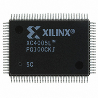
XC4005L-5PQ100C Xilinx Inc, XC4005L-5PQ100C Datasheet - Page 85

XC4005L-5PQ100C
Manufacturer Part Number
XC4005L-5PQ100C
Description
IC 3.3V FPGA 196 CLB'S 100-PQFP
Manufacturer
Xilinx Inc
Series
XC4000r
Datasheet
1.XC4005L-5PC84C.pdf
(175 pages)
Specifications of XC4005L-5PQ100C
Number Of Logic Elements/cells
466
Number Of Labs/clbs
196
Total Ram Bits
6272
Number Of I /o
77
Number Of Gates
5000
Voltage - Supply
3 V ~ 3.6 V
Mounting Type
Surface Mount
Operating Temperature
0°C ~ 85°C
Package / Case
100-BQFP
Lead Free Status / RoHS Status
Contains lead / RoHS non-compliant
Other names
122-1121
Available stocks
Company
Part Number
Manufacturer
Quantity
Price
- Current page: 85 of 175
- Download datasheet (2Mb)
XC4000E CLB Level-Sensitive RAM Switching Characteristic Guidelines
Testing of the switching parameters is modeled after testing methods specified by MIL-M-38510/605. All devices are 100%
functionally tested. Internal timing parameters are not measured directly. They are derived from benchmark timing patterns
that are taken at device introduction, prior to any process improvements. For more detailed, more precise, and more up-to-
date information, use the values provided by the XACT timing calculator and used in the simulator. These values can be
printed in tabular format by running LCA2XNF -S.
The following guidelines reflect worst-case values over the recommended operating conditions. They are expressed in units
of nanoseconds and apply to all XC4000E devices unless otherwise noted.
Note:
September 18, 1996 (Version 1.04)
Write Operation
Address write cycle time
Write Enable pulse width
Address setup time
Address hold time
DIN setup time
DIN hold time
Read Operation
Address read cycle time
Data valid after address
Read Operation, Clocking
Address setup time
Read During Write
Data valid after WE goes
Data valid after DIN
Read During Write, Clock-
WE setup time
Data setup time
after end of WE
before end of WE
after end of WE
(DIN changes during WE)
(High)
before WE
change (no Write Enable)
Data into Flip-Flop
before clock K
active (DIN stable
before WE)
ing Data into Flip-Flop
before clock K
before clock K
Timing for the 16x1 RAM option is identical to 16x2 RAM timing.
Description
Speed Grade
16x2
32x1
16x2
32x1
16x2
32x1
16x2
32x1
16x2
32x1
16x2
32x1
16x2
32x1
16x2
32x1
16x2
32x1
16x2
32x1
16x2
32x1
16x2
32x1
16x2
32x1
Size
Symbol
T
T
T
T
T
T
T
T
T
T
T
T
T
T
T
T
T
T
T
T
T
T
T
T
T
WCKT
T
DCKT
WCT
IHCK
WOT
WCK
WPT
DOT
DCK
AST
AHT
DST
DHT
RCT
IHO
WC
WP
ILO
ICK
WO
DH
RC
DO
AS
AH
DS
Min
8.0
8.0
4.0
4.0
2.0
2.0
2.5
2.0
4.0
5.0
2.0
2.0
4.5
6.5
4.0
6.1
8.0
9.6
7.0
8.0
-4
10.0
12.0
11.0
Max
2.7
4.7
9.0
Min
8.0
8.0
4.0
4.0
2.0
2.0
2.0
2.0
2.2
2.2
2.0
2.0
3.1
5.5
3.0
4.6
6.0
6.8
5.2
6.2
-3
Max
2.0
4.3
6.0
7.3
6.6
7.6
Min
Preliminary
8.0
8.0
4.0
4.0
2.0
2.0
2.0
2.0
0.8
0.8
2.0
2.0
2.6
3.8
2.4
3.9
5.1
5.8
4.4
5.3
-2
Max
1.6
2.7
4.9
5.6
5.8
6.2
4-89
Related parts for XC4005L-5PQ100C
Image
Part Number
Description
Manufacturer
Datasheet
Request
R

Part Number:
Description:
IC 3.3V FPGA 196 CLB'S 84-PLCC
Manufacturer:
Xilinx Inc
Datasheet:

Part Number:
Description:
IC 3.3V FPGA 196 CLB'S 208-PQFP
Manufacturer:
Xilinx Inc
Datasheet:

Part Number:
Description:
IC LOGIC CL ARRAY 5000GAT 160PQF
Manufacturer:
Xilinx Inc
Datasheet:

Part Number:
Description:
IC LOGIC CL ARRAY 5000GAT 208PQ
Manufacturer:
Xilinx Inc
Datasheet:

Part Number:
Description:
IC LOGIC CL ARRAY 5000GAT 84PLC
Manufacturer:
Xilinx Inc
Datasheet:

Part Number:
Description:
FPGA XC4000 Family 5K Gates 196 Cells 100MHz CMOS Technology 5V 160-Pin PQFP
Manufacturer:
Xilinx Inc

Part Number:
Description:
FPGA XC4000 Family 5K Gates 196 Cells 100MHz CMOS Technology 5V 84-Pin PLCC
Manufacturer:
Xilinx Inc

Part Number:
Description:
IC CPLD .8K 36MCELL 44-VQFP
Manufacturer:
Xilinx Inc
Datasheet:

Part Number:
Description:
IC CPLD 72MCRCELL 10NS 44VQFP
Manufacturer:
Xilinx Inc
Datasheet:

Part Number:
Description:
IC CPLD 1.6K 72MCELL 64-VQFP
Manufacturer:
Xilinx Inc
Datasheet:

Part Number:
Description:
IC CR-II CPLD 64MCELL 44-VQFP
Manufacturer:
Xilinx Inc
Datasheet:

Part Number:
Description:
IC CPLD 1.6K 72MCELL 100-TQFP
Manufacturer:
Xilinx Inc
Datasheet:

Part Number:
Description:
IC CR-II CPLD 64MCELL 56-BGA
Manufacturer:
Xilinx Inc
Datasheet:

Part Number:
Description:
IC CPLD 72MCRCELL 7.5NS 44VQFP
Manufacturer:
Xilinx Inc
Datasheet:

Part Number:
Description:
IC CR-II CPLD 64MCELL 100-VQFP
Manufacturer:
Xilinx Inc
Datasheet:


