EP1S40B956C5 Altera, EP1S40B956C5 Datasheet - Page 392
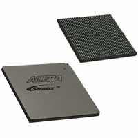
EP1S40B956C5
Manufacturer Part Number
EP1S40B956C5
Description
IC STRATIX FPGA 40K LE 956-BGA
Manufacturer
Altera
Series
Stratix®r
Datasheet
1.EP1S10F484I6N.pdf
(864 pages)
Specifications of EP1S40B956C5
Number Of Logic Elements/cells
41250
Number Of Labs/clbs
4125
Total Ram Bits
3423744
Number Of I /o
683
Voltage - Supply
1.425 V ~ 1.575 V
Mounting Type
Surface Mount
Operating Temperature
0°C ~ 85°C
Package / Case
956-BGA
Lead Free Status / RoHS Status
Contains lead / RoHS non-compliant
Number Of Gates
-
Available stocks
Company
Part Number
Manufacturer
Quantity
Price

Part Number:
EP1S40B956C5
Manufacturer:
ALTERA/阿尔特拉
Quantity:
20 000


Designing With TriMatrix Memory
2–24
Stratix Device Handbook, Volume 2
f
f
f
For information on the difference between APEX-style memory and
TriMatrix memory, see the Transitioning APEX Designs to Stratix Devices
chapter.
Selecting TriMatrix Memory Blocks
The Quartus II software automatically partitions user-defined memory
into embedded memory blocks using the most efficient size
combinations. The memory can also be manually assigned to a specific
block size or a mixture of block sizes.
selecting a TriMatrix memory block size based on supported features.
1
For more information on selecting which memory block to use, see
AN 207: TriMatrix Memory Selection Using the Quartus II Software.
1
Pipeline & Flow-Through Modes
TriMatrix memory architecture implements synchronous (pipelined)
RAM by registering both the input and output signals to the RAM block.
All TriMatrix memory inputs are registered providing synchronous write
cycles. In synchronous operation, RAM generates its own self-timed
strobe write enable (wren) signal derived from the global or regional
clock. In contrast, a circuit using asynchronous RAM must generate the
RAM wren signal while ensuring its data and address signals meet setup
and hold time specifications relative to the wren signal. The output
registers can be bypassed.
In an asynchronous memory neither the input nor the output is
registered. While Stratix and Stratix GX devices do not support
asynchronous memory, they do support a flow-through read where the
output data is available during the clock cycle when the read address is
driven into it. Flow-through reading is possible in the simple and true
dual-port modes of the M512 and M4K blocks by clocking the read enable
and read address registers on the negative clock edge and bypassing the
output registers.
For more information, see AN 210: Converting Memory from Asynchronous
to Synchronous for Stratix & Stratix GX Devices.
Violating the setup or hold time on the address registers could
corrupt the memory contents. This applies to both read and
write operations.
Violating the setup or hold time on the address registers could
corrupt the memory contents. This applies to both read and
write operations.
Table 2–1 on page 2–2
Altera Corporation
is a guide for
July 2005
Related parts for EP1S40B956C5
Image
Part Number
Description
Manufacturer
Datasheet
Request
R

Part Number:
Description:
CYCLONE II STARTER KIT EP2C20N
Manufacturer:
Altera
Datasheet:


Part Number:
Description:
CPLD, EP610 Family, ECMOS Process, 300 Gates, 16 Macro Cells, 16 Reg., 16 User I/Os, 5V Supply, 35 Speed Grade, 24DIP
Manufacturer:
Altera Corporation
Datasheet:
Part Number:
Description:
CPLD, EP610 Family, ECMOS Process, 300 Gates, 16 Macro Cells, 16 Reg., 16 User I/Os, 5V Supply, 15 Speed Grade, 24DIP
Manufacturer:
Altera Corporation
Datasheet:
Part Number:
Description:
Manufacturer:
Altera Corporation
Datasheet:
Part Number:
Description:
CPLD, EP610 Family, ECMOS Process, 300 Gates, 16 Macro Cells, 16 Reg., 16 User I/Os, 5V Supply, 30 Speed Grade, 24DIP
Manufacturer:
Altera Corporation
Datasheet:
Part Number:
Description:
High-performance, low-power erasable programmable logic devices with 8 macrocells, 10ns
Manufacturer:
Altera Corporation
Datasheet:
Part Number:
Description:
High-performance, low-power erasable programmable logic devices with 8 macrocells, 7ns
Manufacturer:
Altera Corporation
Datasheet:
Part Number:
Description:
Classic EPLD
Manufacturer:
Altera Corporation
Datasheet:
Part Number:
Description:
High-performance, low-power erasable programmable logic devices with 8 macrocells, 10ns
Manufacturer:
Altera Corporation
Datasheet:
Part Number:
Description:
Manufacturer:
Altera Corporation
Datasheet:
Part Number:
Description:
Manufacturer:
Altera Corporation
Datasheet:
Part Number:
Description:
Manufacturer:
Altera Corporation
Datasheet:
Part Number:
Description:
CPLD, EP610 Family, ECMOS Process, 300 Gates, 16 Macro Cells, 16 Reg., 16 User I/Os, 5V Supply, 25 Speed Grade, 24DIP
Manufacturer:
Altera Corporation
Datasheet: