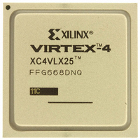
XC4VLX25-11FFG668C Xilinx Inc, XC4VLX25-11FFG668C Datasheet - Page 16

XC4VLX25-11FFG668C
Manufacturer Part Number
XC4VLX25-11FFG668C
Description
IC FPGA VIRTEX-4 24K 668-FCBGA
Manufacturer
Xilinx Inc
Series
Virtex™-4r
Specifications of XC4VLX25-11FFG668C
Number Of Logic Elements/cells
24192
Number Of Labs/clbs
2688
Total Ram Bits
1327104
Number Of I /o
448
Voltage - Supply
1.14 V ~ 1.26 V
Mounting Type
Surface Mount
Operating Temperature
0°C ~ 85°C
Package / Case
668-BBGA, FCBGA
Package
668FCBGA
Family Name
Virtex®-4
Device Logic Units
24192
Typical Operating Supply Voltage
1.2 V
Maximum Number Of User I/os
448
Ram Bits
1327104
For Use With
807-1004 - DAUGHTER CARD WITH VIRTEX-4HW-AFX-FF668-400 - BOARD DEV VIRTEX 4 FF668122-1523 - EVALUATION PLATFORM VIRTEX-4
Lead Free Status / RoHS Status
Lead free / RoHS Compliant
Number Of Gates
-
Other names
122-1490
Available stocks
Company
Part Number
Manufacturer
Quantity
Price
Company:
Part Number:
XC4VLX25-11FFG668C
Manufacturer:
XILINX
Quantity:
101
Company:
Part Number:
XC4VLX25-11FFG668C
Manufacturer:
Xilinx Inc
Quantity:
10 000
Part Number:
XC4VLX25-11FFG668C
Manufacturer:
XILINX/赛灵思
Quantity:
20 000
Table 22: Processor Block APU Interface Switching Characteristics
RocketIO Switching Characteristics
Consult the
Table 23: Maximum RocketIO Transceiver Performance
Table 24: RocketIO Reference Clock Switching Characteristics
DS302 (v3.7) September 9, 2009
Product Specification
Notes:
1.
2.
3.
Setup and Hold Relative to Clock (CPMDFCMCLOCK)
Clock to Out
RocketIO Transceiver
Reference Clock frequency range
GREFCLK Reference Clock frequency range
Reference Clock frequency tolerance
Reference Clock rise time
Reference Clock fall time
Reference Clock duty cycle
Reference Clock total jitter, peak-peak
Clock recovery frequency acquisition time
Spread Spectrum Clocking
APU bus control inputs
APU bus data inputs
APU bus control outputs
APU bus data outputs
MGTCLK input can be used for all serial bit rates. GREFCLK can be used for serial bit rates up to 1 Gb/s.
Measured at the package pin. For serial rates equal to or above 1 Gb/s, MGTCLK must be used. UI = Unit Interval.
Tested with synchronous reference clock.
Virtex-4 RocketIO Multi-Gigabit Transceiver User Guide
Description
Description
80%
20%
(3)
Description
T
(1)
FCLK
(2)
Figure 3: Reference Clock Timing Parameters
(1)
F
Symbol
T
GREFCLK
F
T
F
T
T
T
DCREF
GCLK
GTOL
LOCK
RCLK
FCLK
GJTT
T
T
T
T
T
T
PPCDCK
PPCCKD
PPCDCK
PPCCKD
PPCCKO
PPCCKO
T
www.xilinx.com
RCLK
Virtex-4 FPGA Data Sheet: DC and Switching Characteristics
CLK
CLK
CLK
20% – 80%
20% – 80%
CLK
CLK
Initial lock of the PLL from
startup (programmable)
0% to –0.5%
Symbol
_DCDCREN
_DCDCREN
_RESULT
_RESULT
_APUFCMDEC
_RADATA
Conditions
for further information.
-12
6.5
0.33
0.20
0.61
0.20
1.53
1.53
-12
Speed Grade
Speed Grade
DS302_04_031708
-11
6.5
–350
Min
106
106
106
45
30
0.36
0.20
0.67
0.20
1.75
1.75
-11
-11/-12 Speed Grades
All Speed Grades
-10 Speed Grade
Typ
1
3.125
-10
0.42
0.23
0.78
0.23
2.00
2.00
-10
+350
Max
400
644
320
400
400
55
40
33
ns, Max
ns, Max
ns, Min
ns, Min
Units
Units
Units
Gb/s
MHz
MHz
MHz
ppm
kHz
ms
ps
ps
ps
%
16


