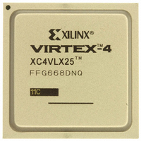
XC4VLX25-11FFG668C Xilinx Inc, XC4VLX25-11FFG668C Datasheet - Page 57

XC4VLX25-11FFG668C
Manufacturer Part Number
XC4VLX25-11FFG668C
Description
IC FPGA VIRTEX-4 24K 668-FCBGA
Manufacturer
Xilinx Inc
Series
Virtex™-4r
Specifications of XC4VLX25-11FFG668C
Number Of Logic Elements/cells
24192
Number Of Labs/clbs
2688
Total Ram Bits
1327104
Number Of I /o
448
Voltage - Supply
1.14 V ~ 1.26 V
Mounting Type
Surface Mount
Operating Temperature
0°C ~ 85°C
Package / Case
668-BBGA, FCBGA
Package
668FCBGA
Family Name
Virtex®-4
Device Logic Units
24192
Typical Operating Supply Voltage
1.2 V
Maximum Number Of User I/os
448
Ram Bits
1327104
For Use With
807-1004 - DAUGHTER CARD WITH VIRTEX-4HW-AFX-FF668-400 - BOARD DEV VIRTEX 4 FF668122-1523 - EVALUATION PLATFORM VIRTEX-4
Lead Free Status / RoHS Status
Lead free / RoHS Compliant
Number Of Gates
-
Other names
122-1490
Available stocks
Company
Part Number
Manufacturer
Quantity
Price
Company:
Part Number:
XC4VLX25-11FFG668C
Manufacturer:
XILINX
Quantity:
101
Company:
Part Number:
XC4VLX25-11FFG668C
Manufacturer:
Xilinx Inc
Quantity:
10 000
Part Number:
XC4VLX25-11FFG668C
Manufacturer:
XILINX/赛灵思
Quantity:
20 000
DS302 (v3.7) September 9, 2009
Product Specification
09/28/07
12/11/07
04/10/08
06/06/08
11/26/08
06/16/09
08/13/09
09/09/09
Date
Version
3.0
3.1
3.2
3.3
3.4
3.5
3.6
3.7
•
•
•
•
•
•
•
•
•
•
•
•
•
•
•
•
•
•
•
•
•
•
•
•
•
•
•
•
•
•
SPEED SPECIFICATION version for this data sheet release: v1.67.
Promoted data sheet to Production status.
Table
Table
adding “vertical”.
Table
Table
SPEED SPECIFICATION version for this data sheet release: v1.68.
Added new copyright notice and legal disclaimer section.
Table
(obsolete). Renumbered table notes.
Table
Table
Table
Table
LVDSEXT_25.
Table
Table
Table
Section
by the ISE tool in the PAR report.
SPEED SPECIFICATION version for this data sheet release: v1.68.
Table 28, page
Table 43, page
Table 63, page
SPEED SPECIFICATION version for this data sheet release: v1.68.
Table 3, page
maximum I
Table 24, page
on the speed grade. Removed T
Table 35, page
Table 35, page
Table 40, page
Table 3, page
Table 45, page
CLKIN_FREQ_DLL_HF_MS_MIN and CLKIN_FREQ_FX_HF_MS_MAX.
Table 7, page
14: Moved XC4VFX140, all speed grades, from Advance to Production status.
59: Added/updated all Global Clock Tree Skew values. Qualified Note (2) by
60: Added Package Skew values for XC4VFX40, XC4VFX100, and XC4VFX140.
63: Added JTAG ID code for XC4VFX140.
13: Removed table note references to XAPP700, XAPP704, and XAPP705
15: Added new Note 1, renumbered subsequent table notes.
30: Removed table rows for LVPECL_33, LVDS_33, and LVDSEXT_33.
30,
31: For LVDS Extended Mode 2.5V, corrected I/O Standard Attribute to
37: Added Note 4 specifying F
43: Added parameter F
58: Corrected T
Production Stepping, page
Table
CC
3: In Note (2), clarified differences between settings for typical and
3: Updated Note 1.
8: Added “LVCMOS” to Notes 3 and 4.
numbers.
22: Re-inserted table.
36: Updated Symbol names for the DRP entries.
51: Revised code for XC4VFX40 package to 0.
16: Revised
29: Reorganized according to IDELAYCTRL and IDELAY.
29: Added F
33: Changed T
38: Added Note 6 reference to and updated descriptions of
31: Corrected “electron-coupled” to “emitter-coupled”.
www.xilinx.com
PSFD
Virtex-4 FPGA Data Sheet: DC and Switching Characteristics
for XC4VFX100 devices to 1.99 ns.
MAX
F
MAX_READBACK
GCLK
RCKO_DOA
.
PHASE
to show different maximum frequencies depending
Revisions
TOG
51: Advised that current stepping level is reported
.
for -11 FX devices as 1181 MHz.
to a Max parameter.
.
57


