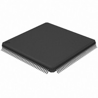
AT94K05AL-25BQU Atmel, AT94K05AL-25BQU Datasheet - Page 174

AT94K05AL-25BQU
Manufacturer Part Number
AT94K05AL-25BQU
Description
IC FPSLIC 5K GATE 25MHZ 144-LQFP
Manufacturer
Atmel
Series
FPSLIC®r
Datasheet
1.AT94K05AL-25AJI.pdf
(204 pages)
Specifications of AT94K05AL-25BQU
Core Type
8-bit AVR
Speed
25MHz
Interface
I²C, UART
Program Sram Bytes
4K-16K
Fpga Sram
2kb
Data Sram Bytes
4K ~ 16K
Fpga Core Cells
256
Fpga Gates
5K
Fpga Registers
436
Voltage - Supply
3 V ~ 3.6 V
Mounting Type
Surface Mount
Operating Temperature
-40°C ~ 85°C
Package / Case
144-LQFP
For Use With
ATSTK594 - BOARD FPSLIC DAUGHTER FOR STK500
Lead Free Status / RoHS Status
Lead free / RoHS Compliant
Eeprom Size
-
Available stocks
Company
Part Number
Manufacturer
Quantity
Price
- Current page: 174 of 204
- Download datasheet (4Mb)
6.1.1
Table 6-2.
Table 6-3.
174
Symbol
t
t
t
t
t
t
t
Symbol
t
t
t
t
t
t
ADS
ADH
RDS
RDH
ACC
MEH
MEl
ADS
ADH
WRS
MPW
WDS
WDH
AT94KAL Series FPSLIC
Frame Interface
Parameter
Address Setup
Address Hold
Read Cycle Setup
Read Cycle Hold
Access Time from Posedge ME
Minimum ME High
Minimum ME Low
Parameter
Address Setup
Address Hold
Write Cycle Setup
Minimum Write Duration
Data Setup to Write End
Data Hold to Write End
SRAM Read Cycle Timing Numbers
Commercial 3.3V ± 10%/Industrial 3.3V ± 10%
SRAM Write Cycle Timing Numbers
Commercial 3.3V ± 10%/Industrial 3.3V ± 10%
The FPGA Frame Clock phase is selectable (see
page
relation of ME to data, address and write enable does not change). By default, FrameClock is
inverted (ME = ~FrameClock). Selecting the non-inverted phase assigns ME = FrameClock.
Recall, the Dual-port SRAM operates in single-edge clock controlled mode during read opera-
tions, and double-edge clock controlled mode during writes. Addresses are clocked internally on
the rising edge of the clock signal (ME). Any change of address without a rising edge of ME is
not considered.
30). This document refers to the clock at the FPGA/Dual-port SRAM interface as ME (the
Minimum
Minimum
0.6
0.7
3.4
0.7
0.6
0.6
0.7
1.4
4.6
0.6
0
0
0
Commercial
Commercial
Typical
Typical
0.8
0.9
4.2
0.9
0.8
0.8
0.9
1.8
5.7
0.8
0
0
0
Maximum
Maximum
1.1
1.3
5.9
1.1
1.3
8.0
1.3
1.1
2.5
1.1
0
0
0
“System Control Register – FPGA/AVR” on
Minimum
Minimum
0.5
0.6
2.9
0.6
0.6
0.5
0.6
1.2
3.9
0.5
0
0
0
Industrial
Industrial
Typical
Typical
0.8
0.9
4.2
0.9
0.8
0.8
0.9
1.8
5.7
0.8
0
0
0
Maximum
Maximum
1.2
1.5
6.9
1.5
1.2
1.5
3.0
1.3
9.4
1.3
0
0
0
1138I–FPSLI–1/08
Units
Units
ns
ns
ns
ns
ns
ns
ns
ns
ns
ns
ns
ns
ns
Related parts for AT94K05AL-25BQU
Image
Part Number
Description
Manufacturer
Datasheet
Request
R

Part Number:
Description:
IC FPSLIC 5K GATE 25MHZ 84PLCC
Manufacturer:
Atmel
Datasheet:

Part Number:
Description:
Fpslic Devices Combine 5K Gates of Atmel's Patented AT40K Fpga Architecture, a 20 Mips Avr 8-bit Risc Microprocessor Core, Numerous Fixed Microcontroller Peripheries And up to 36K Bytes of Program And Data SRAM.
Manufacturer:
ATMEL Corporation
Datasheet:

Part Number:
Description:
IC FPSLIC 5K GATE 25MHZ 84PLCC
Manufacturer:
Atmel
Datasheet:

Part Number:
Description:
IC FPSLIC 5K GATE 25MHZ 208PQFP
Manufacturer:
Atmel
Datasheet:

Part Number:
Description:
IC FPSLIC 5K GATE 25MHZ 144LQFP
Manufacturer:
Atmel
Datasheet:

Part Number:
Description:
IC FPSLIC 5K GATE 25MHZ 208PQFP
Manufacturer:
Atmel
Datasheet:

Part Number:
Description:
IC FPSLIC 5K GATE 25MHZ 144LQFP
Manufacturer:
Atmel
Datasheet:

Part Number:
Description:
IC FPSLIC 5K GATE 25MHZ 100-TQFP
Manufacturer:
Atmel
Datasheet:

Part Number:
Description:
Manufacturer:
Atmel
Datasheet:

Part Number:
Description:
Manufacturer:
Atmel
Datasheet:

Part Number:
Description:
Manufacturer:
Atmel
Datasheet:

Part Number:
Description:
5k - 40k Gates Of At40k Fpga With 8-bit Microcontroller, Up To 36k Bytes Of Sram And On-chip Jtag Ice
Manufacturer:
ATMEL Corporation
Datasheet:

Part Number:
Description:
At94k05al 5k - 40k Gates Of At40k Fpga With 8-bit Microcontroller, Up To 36k Bytes Of Sram And On-chip Jtag Ice
Manufacturer:
ATMEL Corporation
Datasheet:

Part Number:
Description:
DEV KIT FOR AVR/AVR32
Manufacturer:
Atmel
Datasheet:


