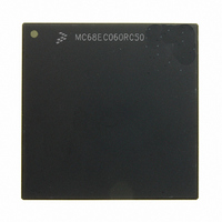
MC68EC060RC50 Freescale Semiconductor, MC68EC060RC50 Datasheet - Page 184

MC68EC060RC50
Manufacturer Part Number
MC68EC060RC50
Description
IC MPU 32BIT 50MHZ 206-PGA
Manufacturer
Freescale Semiconductor
Specifications of MC68EC060RC50
Processor Type
M680x0 32-Bit
Speed
50MHz
Voltage
3.3V
Mounting Type
Surface Mount
Package / Case
206-PGA
Family Name
M68000
Device Core
ColdFire
Device Core Size
32b
Frequency (max)
50MHz
Instruction Set Architecture
RISC
Supply Voltage 1 (typ)
3.3V
Operating Supply Voltage (max)
3.465V
Operating Supply Voltage (min)
3.135V
Operating Temp Range
0C to 110C
Operating Temperature Classification
Commercial
Mounting
Through Hole
Pin Count
206
Package Type
PGA
Lead Free Status / RoHS Status
Contains lead / RoHS non-compliant
Features
-
Lead Free Status / Rohs Status
Compliant
Available stocks
Company
Part Number
Manufacturer
Quantity
Price
Company:
Part Number:
MC68EC060RC50
Manufacturer:
NXP
Quantity:
1 746
- Current page: 184 of 416
- Download datasheet (2Mb)
read-modify-write sequence, the MC68060 asserts the LOCK signal to indicate that an indi-
visible operation is occurring and asserts the LOCKE signal for the last write bus cycle to
indicate completion of the locked sequence. In addition to LOCK and LOCKE, the MC68060
provides the BGR input to allow external arbiters to indicate to the processor whether or not
to break a locked sequence. Refer to 7.11 Bus Arbitration for details on the bus arbitration
protocol.
The external arbiter can use the LOCK, LOCKE, and/or BGR to prevent arbitration of the
bus during locked processor sequences. External bus arbitrations can use LOCKE to sup-
port bus arbitration between consecutive read-modify-write cycles. A read-modify-write
operation is treated as noncachable. If the access hits in the data cache, it invalidates a
matching valid entry and pushes a matching dirty entry. The read-modify-write transfer
begins after the line push (if required) is complete; however, LOCK may assert during the
line push bus cycle.
The TAS, CAS, and MOVEC of BUSCR instructions are the only MC68060 instructions that
utilize read-modify-write transfers. Some page descriptor updates during translation table
searches also use read-modify-write transfers. Refer to Section 4 Memory Management
Unit for information about table searches.
The read-modify-write transfer for the CAS instruction in the MC68060 is similar to that of
the MC68040. If an operand does not match one of these instructions, the MC68060 exe-
cutes a single write transfer to terminate the locked sequence with LOCKE asserted. For the
CAS instruction, the value read from memory is written back. Figure 7-23 illustrates a func-
tional timing diagram for a TAS instruction read-modify-write bus transfer.
Clock 1 (C1)
Clock 2 (C2)
MOTOROLA
The read cycle starts in C1. During C1, the processor places valid values on the address
bus and transfer attributes. LOCK is asserted to identify a locked read-modify-write bus
cycle. For user and supervisor mode accesses, which the corresponding memory unit
translates, the UPAx signals are driven with the values from the matching U1 and U0 bits.
The TTx and TMx signals identify the specific access type. R/W is driven high for a read
cycle. CIOUT is asserted if the access is identified as noncachable. The processor asserts
TS during C1 to indicate the beginning of a bus cycle. If not already asserted from a pre-
vious bus cycle, the TIP signal is also asserted at this time to indicate that a bus cycle is
active. Refer to Section 4 Memory Management Unit for information on the MC68060
and MC68LC060 memory units and Appendix B MC68EC060 for information on the
MC68EC060 memory unit.
During C2, the processor negates TS. The selected device uses R/W, SIZ1, SIZ0, A1, and
A0 or BSx, to place its information on the data bus. With the exception of R/W, these sig-
nals also select any or all of the data bus bytes (D24–D31, D16–D23, D15–D8, and D7–
D0).
Concurrently, the selected device asserts TA. At the end of the C2, assuming that the ac-
knowledge termination ignore state capability is disabled, the processor samples the level
of TA and registers the current value on the data bus. If TA is asserted, the read transfer
terminates and the registered data is passed to the appropriate memory unit. If TA is not
M68060 USER’S MANUAL
Bus Operation
7-29
Related parts for MC68EC060RC50
Image
Part Number
Description
Manufacturer
Datasheet
Request
R
Part Number:
Description:
Manufacturer:
Freescale Semiconductor, Inc
Datasheet:
Part Number:
Description:
Manufacturer:
Freescale Semiconductor, Inc
Datasheet:
Part Number:
Description:
Manufacturer:
Freescale Semiconductor, Inc
Datasheet:
Part Number:
Description:
Manufacturer:
Freescale Semiconductor, Inc
Datasheet:
Part Number:
Description:
Manufacturer:
Freescale Semiconductor, Inc
Datasheet:
Part Number:
Description:
Manufacturer:
Freescale Semiconductor, Inc
Datasheet:
Part Number:
Description:
Manufacturer:
Freescale Semiconductor, Inc
Datasheet:
Part Number:
Description:
Manufacturer:
Freescale Semiconductor, Inc
Datasheet:
Part Number:
Description:
Manufacturer:
Freescale Semiconductor, Inc
Datasheet:
Part Number:
Description:
Manufacturer:
Freescale Semiconductor, Inc
Datasheet:
Part Number:
Description:
Manufacturer:
Freescale Semiconductor, Inc
Datasheet:
Part Number:
Description:
Manufacturer:
Freescale Semiconductor, Inc
Datasheet:
Part Number:
Description:
Manufacturer:
Freescale Semiconductor, Inc
Datasheet:
Part Number:
Description:
Manufacturer:
Freescale Semiconductor, Inc
Datasheet:
Part Number:
Description:
Manufacturer:
Freescale Semiconductor, Inc
Datasheet:


