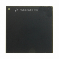
MC68EC060RC50 Freescale Semiconductor, MC68EC060RC50 Datasheet - Page 267

MC68EC060RC50
Manufacturer Part Number
MC68EC060RC50
Description
IC MPU 32BIT 50MHZ 206-PGA
Manufacturer
Freescale Semiconductor
Specifications of MC68EC060RC50
Processor Type
M680x0 32-Bit
Speed
50MHz
Voltage
3.3V
Mounting Type
Surface Mount
Package / Case
206-PGA
Family Name
M68000
Device Core
ColdFire
Device Core Size
32b
Frequency (max)
50MHz
Instruction Set Architecture
RISC
Supply Voltage 1 (typ)
3.3V
Operating Supply Voltage (max)
3.465V
Operating Supply Voltage (min)
3.135V
Operating Temp Range
0C to 110C
Operating Temperature Classification
Commercial
Mounting
Through Hole
Pin Count
206
Package Type
PGA
Lead Free Status / RoHS Status
Contains lead / RoHS non-compliant
Features
-
Lead Free Status / Rohs Status
Compliant
Available stocks
Company
Part Number
Manufacturer
Quantity
Price
Company:
Part Number:
MC68EC060RC50
Manufacturer:
NXP
Quantity:
1 746
- Current page: 267 of 416
- Download datasheet (2Mb)
IEEE 1149.1 Test (JTAG) and Debug Pipe Control Modes
through at least five rising edges and the falling edge after the fifth rising edge. A JTAG reset
will cause the TAP state machine to enter the test-logic-reset state (normal operation of the
TAP state machine into the test-logic-reset state will also result in placing the default value
of $5 into the instruction register). The shift register portion of the instruction register is
loaded with the default value of $5 when in the Capture-IR state and a rising edge of TCK
occurs.
9.1.2.6 CLAMP. The CLAMP instruction selects the bypass register while simultaneously
forcing all output pins and bidirectional pins configured as outputs, to the fixed values that
are preloaded and held in the boundary scan update registers. This instruction enhances
test efficiency by reducing the overall shift path to a single bit (the bypass register) while con-
ducting an EXTEST type of instruction through the boundary scan register. The CLAMP
instruction becomes active on the falling edge of TCK in the update-IR state when the data
held in the instruction shift register is equivalent to $6.
It is recommended that the boundary scan register bit equivalent to the RSTI pin be pre-
loaded with the assert value for system reset prior to application of the CLAMP instruction.
This will ensure that CLAMP asserts the internal reset for the MC68060 system logic to force
a predictable benign internal state while isolating all pins from signals generated external to
the part. However, if it is desired to hold the processor in the LPSTOP state when applying
the CLAMP instruction, do not preload the boundary scan register bit equivalent to the RSTI
pin with an assert value because this action forces the processor out of the LPSTOP state.
9.1.2.7 HIGHZ. The HIGHZ instruction is an IEEE 1149.1 option that is provided as a Motor-
ola public instruction designed to anticipate the need to backdrive the output pins and pro-
tect the input pins from random toggling during circuit board testing. The HIGHZ instruction
selects the bypass register, forces all output and bidirectional pins to the high-impedance
state, and isolates all input signal pins except for CLK, IPL, and RSTI. The HIGHZ instruction
becomes active on the falling edge of TCK in the update-IR state when the data held in the
instruction shift register is equivalent to $7.
It is recommended that the boundary scan register bit equivalent to the RSTI pin be pre-
loaded with the assert value for system reset prior to application of the HIGHZ instruction.
This will ensure that HIGHZ asserts the internal reset for the MC68060 system logic to force
a predictable benign internal state while isolating all pins from signals generated external to
the part.
9.1.2.8 BYPASS. The BYPASS instruction selects the single-bit bypass register, creating a
single bit shift register path from the TDI pin to the bypass register to the TDO pin. This
instruction enhances test efficiency by reducing the overall shift path when a device other
than the MC68060 becomes the device under test on a board design with multiple chips on
the overall IEEE-1149.1-defined boundary scan chain. The bypass register has been imple-
mented in accordance with IEEE 1149.1 so that the shift register stage is set to logic zero
on the rising edge of TCK following entry into the capture-DR state. Therefore, the first bit
to be shifted out after selecting the bypass register is always a logic zero (this is to differen-
tiate a part that supports an idcode register from a part that supports only the bypass regis-
ter).
9-6
M68060 USER’S MANUAL
MOTOROLA
Related parts for MC68EC060RC50
Image
Part Number
Description
Manufacturer
Datasheet
Request
R
Part Number:
Description:
Manufacturer:
Freescale Semiconductor, Inc
Datasheet:
Part Number:
Description:
Manufacturer:
Freescale Semiconductor, Inc
Datasheet:
Part Number:
Description:
Manufacturer:
Freescale Semiconductor, Inc
Datasheet:
Part Number:
Description:
Manufacturer:
Freescale Semiconductor, Inc
Datasheet:
Part Number:
Description:
Manufacturer:
Freescale Semiconductor, Inc
Datasheet:
Part Number:
Description:
Manufacturer:
Freescale Semiconductor, Inc
Datasheet:
Part Number:
Description:
Manufacturer:
Freescale Semiconductor, Inc
Datasheet:
Part Number:
Description:
Manufacturer:
Freescale Semiconductor, Inc
Datasheet:
Part Number:
Description:
Manufacturer:
Freescale Semiconductor, Inc
Datasheet:
Part Number:
Description:
Manufacturer:
Freescale Semiconductor, Inc
Datasheet:
Part Number:
Description:
Manufacturer:
Freescale Semiconductor, Inc
Datasheet:
Part Number:
Description:
Manufacturer:
Freescale Semiconductor, Inc
Datasheet:
Part Number:
Description:
Manufacturer:
Freescale Semiconductor, Inc
Datasheet:
Part Number:
Description:
Manufacturer:
Freescale Semiconductor, Inc
Datasheet:
Part Number:
Description:
Manufacturer:
Freescale Semiconductor, Inc
Datasheet:


