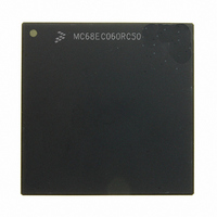
MC68EC060RC50 Freescale Semiconductor, MC68EC060RC50 Datasheet - Page 304

MC68EC060RC50
Manufacturer Part Number
MC68EC060RC50
Description
IC MPU 32BIT 50MHZ 206-PGA
Manufacturer
Freescale Semiconductor
Specifications of MC68EC060RC50
Processor Type
M680x0 32-Bit
Speed
50MHz
Voltage
3.3V
Mounting Type
Surface Mount
Package / Case
206-PGA
Family Name
M68000
Device Core
ColdFire
Device Core Size
32b
Frequency (max)
50MHz
Instruction Set Architecture
RISC
Supply Voltage 1 (typ)
3.3V
Operating Supply Voltage (max)
3.465V
Operating Supply Voltage (min)
3.135V
Operating Temp Range
0C to 110C
Operating Temperature Classification
Commercial
Mounting
Through Hole
Pin Count
206
Package Type
PGA
Lead Free Status / RoHS Status
Contains lead / RoHS non-compliant
Features
-
Lead Free Status / Rohs Status
Compliant
Available stocks
Company
Part Number
Manufacturer
Quantity
Price
Company:
Part Number:
MC68EC060RC50
Manufacturer:
NXP
Quantity:
1 746
- Current page: 304 of 416
- Download datasheet (2Mb)
Instruction Execution Timing
Additionally, the use of instruction folding techniques allow one or two instructions to be
simultaneously executed with a predicted taken Bcc (also for BRA and JMP instructions).
The floating-point pre-exception model of the MC68060 supports execution overlap
between multi-cycle floating-point instructions and the integer execute engines. Once a
multi-cycle floating-point instruction has started its execution, the primary and secondary
OEPs may continue to dispatch and complete integer instructions in parallel with the
floating-point instructions. The OEPs will stall only if another floating-point instruction is
encountered before the first floating-point instruction has completed its execution. The
floating-point instructions that permit this execution overlap are classified as pOEP-but-
allows-sOEP in Table 10-4.
10.1.3 Dispatch Test 3: Allowable Effective Addressing Mode in the sOEP
To minimize the hardware structures required for the address generation unit within the sec-
ondary OEP, certain addressing modes are not allowed. The addressing modes not sup-
ported by the sOEP include: the address register indirect with index plus base displacement
{(bd, An, Xi SF)} and all PC-relative modes {(d16, PC), (d8, PC, Xi SF), (bd, PC, Xi SF)}.
10.1.4 Dispatch Test 4: Allowable Operand Data Memory Reference
The MC68060 processor design features a shared operand data cache pipeline capable of
supporting a single operand reference per machine cycle. This test validates that only a sin-
gle operand data memory reference is present between the instruction-pair in the pOEP and
sOEP.
10.1.5 Dispatch Test 5: No Register Conflicts on sOEP.AGU Resources
This test validates that the register resources of the sOEP.AGU (Base, Index) do not conflict
with the results being generated by the instruction in the pOEP. The most significant bit of
the resource name is asserted to indicate a register resource. Thus, this test can be stated
as:
As examples of failing sequences, consider the following instruction pairs:
10-8
test5 = 1
if (sOEP.Base > 15)/* indicates a valid register
/* if the sOEP.Base equals the pOEP’s Address_ or Execute_result, a conflict exists
if (sOEP.Index > 15)/* indicates a valid register
/* if the sOEP.Index equals the pOEP’s Address_ or Execute_result, a conflict exists
if ((sOEP.Base = pOEP.Address_result) || (sOEP.Base = pOEP.Execute_result))
if ((sOEP.Index = pOEP.Address_result) || (sOEP.Index = pOEP.Execute_result))
add.l #<data>,a0Execute_result = a0
mov.l (a0),d0Base = a0
add.l d1,d0 Execute_result = d0
lea
test5 = 0/* test5 has register conflict; test fails
test5 = 0/* test5 has register conflict; test fails
(a1,d0.l),a0Index = d0
/* set test5 as okay
M68060 USER’S MANUAL
MOTOROLA
Related parts for MC68EC060RC50
Image
Part Number
Description
Manufacturer
Datasheet
Request
R
Part Number:
Description:
Manufacturer:
Freescale Semiconductor, Inc
Datasheet:
Part Number:
Description:
Manufacturer:
Freescale Semiconductor, Inc
Datasheet:
Part Number:
Description:
Manufacturer:
Freescale Semiconductor, Inc
Datasheet:
Part Number:
Description:
Manufacturer:
Freescale Semiconductor, Inc
Datasheet:
Part Number:
Description:
Manufacturer:
Freescale Semiconductor, Inc
Datasheet:
Part Number:
Description:
Manufacturer:
Freescale Semiconductor, Inc
Datasheet:
Part Number:
Description:
Manufacturer:
Freescale Semiconductor, Inc
Datasheet:
Part Number:
Description:
Manufacturer:
Freescale Semiconductor, Inc
Datasheet:
Part Number:
Description:
Manufacturer:
Freescale Semiconductor, Inc
Datasheet:
Part Number:
Description:
Manufacturer:
Freescale Semiconductor, Inc
Datasheet:
Part Number:
Description:
Manufacturer:
Freescale Semiconductor, Inc
Datasheet:
Part Number:
Description:
Manufacturer:
Freescale Semiconductor, Inc
Datasheet:
Part Number:
Description:
Manufacturer:
Freescale Semiconductor, Inc
Datasheet:
Part Number:
Description:
Manufacturer:
Freescale Semiconductor, Inc
Datasheet:
Part Number:
Description:
Manufacturer:
Freescale Semiconductor, Inc
Datasheet:


