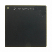
MC68EC060RC50 Freescale Semiconductor, MC68EC060RC50 Datasheet - Page 368

MC68EC060RC50
Manufacturer Part Number
MC68EC060RC50
Description
IC MPU 32BIT 50MHZ 206-PGA
Manufacturer
Freescale Semiconductor
Specifications of MC68EC060RC50
Processor Type
M680x0 32-Bit
Speed
50MHz
Voltage
3.3V
Mounting Type
Surface Mount
Package / Case
206-PGA
Family Name
M68000
Device Core
ColdFire
Device Core Size
32b
Frequency (max)
50MHz
Instruction Set Architecture
RISC
Supply Voltage 1 (typ)
3.3V
Operating Supply Voltage (max)
3.465V
Operating Supply Voltage (min)
3.135V
Operating Temp Range
0C to 110C
Operating Temperature Classification
Commercial
Mounting
Through Hole
Pin Count
206
Package Type
PGA
Lead Free Status / RoHS Status
Contains lead / RoHS non-compliant
Features
-
Lead Free Status / Rohs Status
Compliant
Available stocks
Company
Part Number
Manufacturer
Quantity
Price
Company:
Part Number:
MC68EC060RC50
Manufacturer:
NXP
Quantity:
1 746
- Current page: 368 of 416
- Download datasheet (2Mb)
For most systems, the entry-points _isp_cas() and _isp_cas2() routines should provide suf-
ficient emulation results. However, it is up to the system integrator to judge whether or not
these routines are sufficient, or that a more system-specific solution is needed. The following
is a description of some aspects of the _isp_cas() and _isp_cas2() emulation code.
MOTOROLA
3. After emulation is completed, the pages which may have been “locked” from being
1. Interrupt levels 0-6 are immediately masked. If the appropriate pages have been
2. The operand ATC is loaded for each operand using the PLPAW instruction. In addi-
3. The main algorithm steps are pre-fetched into the instruction cache if the cache is en-
4. Before performing the read(s)/write(s), the bus LOCK signal is asserted by the emula-
5. The LOCKE signal will be asserted for the final operand write of the emulation se-
6. The actual read(s)/write(s) are performed using the MOVES instruction for both user
system-specific solution, then the new user-generated emulation code should supply
the routines via the _real_cas()/_real_cas2() call-outs, and should then re-enter the
MC68060ISP through the entry point _isp_cas_finish() or _isp_cas2_finish() when
complete.
paged out earlier must now be “unlocked”. To accomplish this, the MC68060ISP exe-
cutes a _real_unlock_page() call-out for each operand.
paged in and have been checked for write permission in _real_lock_page(), then only
physical bus errors can occur within this code sequence. The routine restores the pre-
vious interrupt mask level upon completion of the algorithm. (Note: if a system, by de-
sign, allows level 7 interrupts to occur while emulating the CAS or CAS2 instructions,
then the operand data corruption may occur. External hardware may be added to the
system to physically mask all interrupts whenever LOCK is asserted.)
tion, any fresh cache entries corresponding to the operands are pushed from the
cache using CPUSHL instruction. Note: the MC68040 processor initiated the pushes,
if necessary, within the locked bus region. MC68060 hardware, however, pushes the
cache lines, if necessary, outside of the locked bus region for TAS and aligned CAS
instructions. The MC68060ISP emulates the MC68060 processor approach.
abled. The algorithm attempts to allow only operand data bus accesses during the
locked bus instruction sequence. This strategy reduces the number of cycles that the
LOCK signal will be asserted.
tion code by using the MOVEC of the BUSCR register. All reads and writes when
LOCK is asserted will be precise. LOCK will not actually appear on the bus until the
first bus read cycle.
quence.
and supervisor accesses. The system DFC is set to the appropriate mode before ex-
ecuting MOVES and PLPAW instructions.
M68060 USER’S MANUAL
MC68060 Software Package
C-7
Related parts for MC68EC060RC50
Image
Part Number
Description
Manufacturer
Datasheet
Request
R
Part Number:
Description:
Manufacturer:
Freescale Semiconductor, Inc
Datasheet:
Part Number:
Description:
Manufacturer:
Freescale Semiconductor, Inc
Datasheet:
Part Number:
Description:
Manufacturer:
Freescale Semiconductor, Inc
Datasheet:
Part Number:
Description:
Manufacturer:
Freescale Semiconductor, Inc
Datasheet:
Part Number:
Description:
Manufacturer:
Freescale Semiconductor, Inc
Datasheet:
Part Number:
Description:
Manufacturer:
Freescale Semiconductor, Inc
Datasheet:
Part Number:
Description:
Manufacturer:
Freescale Semiconductor, Inc
Datasheet:
Part Number:
Description:
Manufacturer:
Freescale Semiconductor, Inc
Datasheet:
Part Number:
Description:
Manufacturer:
Freescale Semiconductor, Inc
Datasheet:
Part Number:
Description:
Manufacturer:
Freescale Semiconductor, Inc
Datasheet:
Part Number:
Description:
Manufacturer:
Freescale Semiconductor, Inc
Datasheet:
Part Number:
Description:
Manufacturer:
Freescale Semiconductor, Inc
Datasheet:
Part Number:
Description:
Manufacturer:
Freescale Semiconductor, Inc
Datasheet:
Part Number:
Description:
Manufacturer:
Freescale Semiconductor, Inc
Datasheet:
Part Number:
Description:
Manufacturer:
Freescale Semiconductor, Inc
Datasheet:


