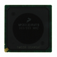
MPC8313EVRAFFB Freescale Semiconductor, MPC8313EVRAFFB Datasheet - Page 38

MPC8313EVRAFFB
Manufacturer Part Number
MPC8313EVRAFFB
Description
IC MPU POWERQUICC II PRO 516PBGA
Manufacturer
Freescale Semiconductor
Datasheet
1.MPC8313CZQAFFB.pdf
(100 pages)
Specifications of MPC8313EVRAFFB
Processor Type
MPC83xx PowerQUICC II Pro 32-Bit
Speed
333MHz
Voltage
0.95 V ~ 1.05 V
Mounting Type
Surface Mount
Package / Case
516-PBGA
Processor Series
MPC8xxx
Core
e300
Data Bus Width
32 bit
Development Tools By Supplier
MPC8313E-RDB
Maximum Clock Frequency
400 MHz
Operating Supply Voltage
- 0.3 V to + 1.26 V
Maximum Operating Temperature
+ 105 C
Mounting Style
SMD/SMT
Data Ram Size
16 KB
I/o Voltage
2.5 V
Interface Type
I2C, SPI, UART
Minimum Operating Temperature
- 40 C
Program Memory Type
EEPROM/Flash
For Use With
MPC8313E-RDB - BOARD PROCESSOR
Lead Free Status / RoHS Status
Lead free / RoHS Compliant
Features
-
Lead Free Status / Rohs Status
Lead free / RoHS Compliant
Available stocks
Company
Part Number
Manufacturer
Quantity
Price
Company:
Part Number:
MPC8313EVRAFFB
Manufacturer:
FREESCAL
Quantity:
150
Company:
Part Number:
MPC8313EVRAFFB
Manufacturer:
Freescale Semiconductor
Quantity:
10 000
High-Speed Serial Interfaces (HSSI)
9.2
The SerDes reference clock inputs are applied to an internal PLL whose output creates the clock used by
the corresponding SerDes lanes. The SerDes reference clocks input is SD_REF_CLK and SD_REF_CLK
for SGMII interface.
The following sections describe the SerDes reference clock requirements and some application
information.
9.2.1
Figure 23
38
•
•
•
•
The supply voltage requirements for XCOREV
SerDes reference clock receiver reference circuit structure:
— The SD_REF_CLK and SD_REF_CLK are internally AC-coupled differential inputs as shown
— The external reference clock driver must be able to drive this termination.
— The SerDes reference clock input can be either differential or single-ended. Refer to the
The maximum average current requirement that also determines the common mode voltage range:
— When the SerDes reference clock differential inputs are DC coupled externally with the clock
— This current limitation sets the maximum common mode input voltage to be less than 0.4 V
— If the device driving the SD_REF_CLK and SD_REF_CLK inputs cannot drive 50 Ω to
The input amplitude requirement. This requirement is described in detail in the following sections.
SerDes Reference Clocks
shows a receiver reference diagram of the SerDes reference clocks.
in
termination to XCOREV
differential mode and single-ended mode description below for further detailed requirements.
driver chip, the maximum average current allowed for each input pin is 8 mA. In this case, the
exact common mode input voltage is not critical as long as it is within the range allowed by the
maximum average current of 8 mA (refer to the following bullet for more detail), since the
input is AC-coupled on-chip.
(0.4 V/50 = 8 mA) while the minimum common mode input level is 0.1 V above XCOREV
For example, a clock with a 50/50 duty cycle can be produced by a clock driver with output
driven by its current source from 0 to 16 mA (0–0.8 V), such that each phase of the differential
input has a single-ended swing from 0 V to 800 mV with the common mode voltage at 400 mV.
XCOREV
AC-coupled off-chip.
SerDes Reference Clock Receiver Characteristics
Figure
MPC8313E PowerQUICC
23. Each differential clock input (SD_REF_CLK or SD_REF_CLK) has a 50-Ω
SS
DC, or it exceeds the maximum input current limitations, then it must be
SS
followed by on-chip AC coupling.
™
II Pro Processor Hardware Specifications, Rev. 3
DD
are specified in
Table 1
and
Freescale Semiconductor
Table
2.
SS
.


