MPC8313EVRAFFB Freescale Semiconductor, MPC8313EVRAFFB Datasheet - Page 46
MPC8313EVRAFFB
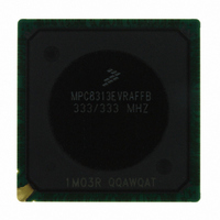
Manufacturer Part Number
MPC8313EVRAFFB
Description
IC MPU POWERQUICC II PRO 516PBGA
Manufacturer
Freescale Semiconductor
Datasheet
1.MPC8313CZQAFFB.pdf
(100 pages)
Specifications of MPC8313EVRAFFB
Processor Type
MPC83xx PowerQUICC II Pro 32-Bit
Speed
333MHz
Voltage
0.95 V ~ 1.05 V
Mounting Type
Surface Mount
Package / Case
516-PBGA
Processor Series
MPC8xxx
Core
e300
Data Bus Width
32 bit
Development Tools By Supplier
MPC8313E-RDB
Maximum Clock Frequency
400 MHz
Operating Supply Voltage
- 0.3 V to + 1.26 V
Maximum Operating Temperature
+ 105 C
Mounting Style
SMD/SMT
Data Ram Size
16 KB
I/o Voltage
2.5 V
Interface Type
I2C, SPI, UART
Minimum Operating Temperature
- 40 C
Program Memory Type
EEPROM/Flash
For Use With
MPC8313E-RDB - BOARD PROCESSOR
Lead Free Status / RoHS Status
Lead free / RoHS Compliant
Features
-
Lead Free Status / Rohs Status
Lead free / RoHS Compliant
Available stocks
Company
Part Number
Manufacturer
Quantity
Price
Company:

Part Number:
MPC8313EVRAFFB
Manufacturer:
FREESCAL
Quantity:
150
Company:
Part Number:
MPC8313EVRAFFB
Manufacturer:
Freescale Semiconductor
Quantity:
10 000


USB
10.1.2
Table 42
Figure 34
10.2
This section describes the DC and AC electrical specifications for the on-chip USB PHY of the
MPC8313E. See Chapter 7 in the USB Specifications Rev. 2, for more information.
46
USB clock cycle time
Input setup to USB clock—all inputs
input hold to USB clock—all inputs
USB clock to output valid—all outputs
Output hold from USB clock—all outputs
Note:
1. The symbols used for timing specifications follow the pattern of t
inputs and t
(USB) for the input (I) to go invalid (X) with respect to the time the USB clock reference (K) goes high (H). Also, t
symbolizes us timing (USB) for the USB clock reference (K) to go high (H), with respect to the output (O) going invalid (X) or
output hold time.
describes the general timing parameters of the USB interface.
On-Chip USB PHY
and
USB AC Electrical Specifications
(first two letters of functional block)(reference)(state)(signal)(state)
Output Signals
USBDR_CLK
Figure 35
Input Signals
MPC8313E PowerQUICC
Parameter
Table 42. USB General Timing Parameters (ULPI Mode Only)
Output
provide the AC test load and signals for the USB, respectively.
t
USKHOV
Figure 34. USB AC Test Load
™
Z
Figure 35. USB Signals
0
II Pro Processor Hardware Specifications, Rev. 3
= 50 Ω
t
USIVKH
t
USKHOX
Symbol
t
t
t
t
USKHOV
USKHOX
USIVKH
USIXKH
t
USCK
(first two letters of functional block)(signal)(state)(reference)(state)
for outputs. For example, t
1
R
L
= 50 Ω
t
USIXKH
Min
15
—
4
1
2
NV
DD
USIXKH
Max
/2
—
—
—
—
7
Freescale Semiconductor
symbolizes USB timing
Unit
ns
ns
ns
ns
ns
USKHOX
Notes
for
Related parts for MPC8313EVRAFFB
Image
Part Number
Description
Manufacturer
Datasheet
Request
R

Part Number:
Description:
Mpc8313e Powerquicc Ii Pro Processor
Manufacturer:
Freescale Semiconductor, Inc
Datasheet:

Part Number:
Description:
BOARD PROCESSOR
Manufacturer:
Freescale Semiconductor
Datasheet:

Part Number:
Description:
BOARD CPU 8313E VER 2.1
Manufacturer:
Freescale Semiconductor
Datasheet:

Part Number:
Description:
BOARD CPU 8313E VER 2.2
Manufacturer:
Freescale Semiconductor
Datasheet:
Part Number:
Description:
Microprocessors - MPU 8313 REV2.2 PB ENC EXT
Manufacturer:
Freescale Semiconductor
Datasheet:
Part Number:
Description:
Microprocessors - MPU 8313 REV2.2 PB W/ENC
Manufacturer:
Freescale Semiconductor
Datasheet:
Part Number:
Description:
Manufacturer:
Freescale Semiconductor, Inc
Datasheet:
Part Number:
Description:
Manufacturer:
Freescale Semiconductor, Inc
Datasheet:
Part Number:
Description:
Manufacturer:
Freescale Semiconductor, Inc
Datasheet:
Part Number:
Description:
Manufacturer:
Freescale Semiconductor, Inc
Datasheet:
Part Number:
Description:
Manufacturer:
Freescale Semiconductor, Inc
Datasheet:
Part Number:
Description:
Manufacturer:
Freescale Semiconductor, Inc
Datasheet:
Part Number:
Description:
Manufacturer:
Freescale Semiconductor, Inc
Datasheet:
Part Number:
Description:
Manufacturer:
Freescale Semiconductor, Inc
Datasheet:
Part Number:
Description:
Manufacturer:
Freescale Semiconductor, Inc
Datasheet: