ADAU1361BCPZ Analog Devices Inc, ADAU1361BCPZ Datasheet - Page 25

ADAU1361BCPZ
Manufacturer Part Number
ADAU1361BCPZ
Description
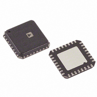
IC CODEC 24B PLL 32LFCSP
Manufacturer
Analog Devices Inc
Type
Audio Codecr
Datasheet
1.ADAU1361BCPZ-RL.pdf
(80 pages)
Specifications of ADAU1361BCPZ
Data Interface
Serial
Resolution (bits)
24 b
Number Of Adcs / Dacs
2 / 2
Sigma Delta
No
Voltage - Supply, Analog
1.8 V ~ 3.6 V
Voltage - Supply, Digital
1.8 V ~ 3.6 V
Operating Temperature
-40°C ~ 85°C
Mounting Type
Surface Mount
Package / Case
32-VFQFN, CSP Exposed Pad
Audio Codec Type
Stereo
No. Of Adcs
2
No. Of Dacs
2
No. Of Input Channels
6
No. Of Output Channels
7
Adc / Dac Resolution
24bit
Adcs / Dacs Signal To Noise Ratio
101dB
Lead Free Status / RoHS Status
Lead free / RoHS Compliant
Available stocks
Company
Part Number
Manufacturer
Quantity
Price
Company:
Part Number:
ADAU1361BCPZ
Manufacturer:
TOSHIBA
Quantity:
1 650
Company:
Part Number:
ADAU1361BCPZ
Manufacturer:
ADI
Quantity:
624
Part Number:
ADAU1361BCPZ
Manufacturer:
ADI/亚德诺
Quantity:
20 000
Part Number:
ADAU1361BCPZ-R7
Manufacturer:
ADI/亚德诺
Quantity:
20 000
Case 2: PLL Is Used
The core clock to the entire chip is off during the PLL lock
acquisition period. The user can poll the lock bit to determine
when the PLL has locked. After lock is acquired, the ADAU1361
can be started by asserting the core clock enable bit (COREN)
in Register R0 (clock control register, Address 0x4000). This bit
enables the core clock to all the internal blocks of the ADAU1361.
PLL Lock Acquisition
During the lock acquisition period, only Register R0 (Address
0x4000) and Register R1 (Address 0x4002) are accessible through
the control port. Because all other registers require a valid master
clock for reading and writing, do not attempt to access any other
register. Any read or write is prohibited until the core clock
enable bit (COREN) and the lock bit are both asserted.
Rev. C | Page 25 of 80
To program the PLL during initialization or reconfiguration of
the clock setting, the following procedure must be followed:
1.
2.
3.
4.
5.
The PLL control register (Register R1, Address 0x4002) is a
48-bit register where all bits must be written with a single
continuous write to the control port.
Power down the PLL.
Reset the PLL control register.
Start the PLL.
Poll the lock bit.
Assert the core clock enable bit after the PLL lock
is acquired.
ADAU1361


