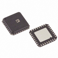
ADAU1361BCPZ Analog Devices Inc, ADAU1361BCPZ Datasheet - Page 26

ADAU1361BCPZ
Manufacturer Part Number
ADAU1361BCPZ
Description
IC CODEC 24B PLL 32LFCSP
Manufacturer
Analog Devices Inc
Type
Audio Codecr
Datasheet
1.ADAU1361BCPZ-RL.pdf
(80 pages)
Specifications of ADAU1361BCPZ
Data Interface
Serial
Resolution (bits)
24 b
Number Of Adcs / Dacs
2 / 2
Sigma Delta
No
Voltage - Supply, Analog
1.8 V ~ 3.6 V
Voltage - Supply, Digital
1.8 V ~ 3.6 V
Operating Temperature
-40°C ~ 85°C
Mounting Type
Surface Mount
Package / Case
32-VFQFN, CSP Exposed Pad
Audio Codec Type
Stereo
No. Of Adcs
2
No. Of Dacs
2
No. Of Input Channels
6
No. Of Output Channels
7
Adc / Dac Resolution
24bit
Adcs / Dacs Signal To Noise Ratio
101dB
Lead Free Status / RoHS Status
Lead free / RoHS Compliant
Available stocks
Company
Part Number
Manufacturer
Quantity
Price
Company:
Part Number:
ADAU1361BCPZ
Manufacturer:
TOSHIBA
Quantity:
1 650
Company:
Part Number:
ADAU1361BCPZ
Manufacturer:
ADI
Quantity:
624
Part Number:
ADAU1361BCPZ
Manufacturer:
ADI/亚德诺
Quantity:
20 000
Part Number:
ADAU1361BCPZ-R7
Manufacturer:
ADI/亚德诺
Quantity:
20 000
ADAU1361
CLOCKING AND SAMPLING RATES
CORE CLOCK
Clocks for the converters and serial ports are derived from the
core clock. The core clock can be derived directly from MCLK
or it can be generated by the PLL. The CLKSRC bit (Bit 3 in
Register R0, Address 0x4000) determines the clock source.
The INFREQ[1:0] bits should be set according to the expected
input clock rate selected by CLKSRC; this value also determines
the core clock rate and the base sampling frequency, f
For example, if the input to CLKSRC = 49.152 MHz (from
PLL), then
The PLL output clock rate is always 1024 × f
control register automatically sets the INFREQ[1:0] bits to
1024 × f
INFREQ[1:0] frequency should be set according to the MCLK
pin clock rate and the desired base sampling frequency.
Table 12. Clock Control Register (Register R0, Address 0x4000)
Bits
3
[2:1]
0
MCLK
INFREQ[1:0] = 1024 × f
f
S
= 49.152 MHz/1024 = 48 kHz
S
Bit Name
CLKSRC
INFREQ[1:0]
COREN
when using the PLL. When using a direct clock, the
R1: PLL CONTROL REGISTER
÷ X
× (R + N/M)
Settings
0: Direct from MCLK pin (default)
1: PLL clock
00: 256 × f
01: 512 × f
10: 768 × f
11: 1024 × f
0: Core clock disabled (default)
1: Core clock enabled
S
S
S
S
(default)
S
CLKSRC
S
CONTROL REGISTER
, and the clock
R0: CLOCK
768 ×
256 ×
INFREQ[1:0]
S
.
f
f
S
S
, 1024 ×
, 512 ×
Figure 29. Clock Tree Diagram
Rev. C | Page 26 of 80
f
S
f
S
,
CLOCK
CORE
SAMPLING RATES
The ADCs, DACs, and serial port share a common sampling
rate that is set in Register R17 (Converter Control 0 register,
Address 0x4017). The CONVSR[2:0] bits set the sampling rate
as a ratio of the base sampling frequency.
Table 13 and Table 14 list the sampling rate divisions for
common base sampling rates.
Table 13. 48 kHz Base Sampling Rate Divisions
Base Sampling
Frequency
f
Table 14. 44.1 kHz Base Sampling Rate Divisions
Base Sampling
Frequency
f
CONTROL 0 REGISTER
S
S
f
S
= 48 kHz
= 44.1 kHz
R17: CONVERTER
/0.5, 1, 1.5, 2, 3, 4, 6
CONVSR[2:0]
Sampling Rate Scaling
f
f
f
f
f
f
f
Sampling Rate Scaling
f
f
f
f
f
f
f
S
S
S
S
S
S
S
S
S
S
S
S
S
S
/1
/6
/4
/3
/2
/1.5
/0.5
/1
/6
/4
/3
/2
/1.5
/0.5
ADCs
DACs
Sampling Rate
48 kHz
8 kHz
12 kHz
16 kHz
24 kHz
32 kHz
96 kHz
Sampling Rate
44.1 kHz
7.35 kHz
11.025 kHz
14.7 kHz
22.05 kHz
29.4 kHz
88.2 kHz
INPUT/OUTPUT
SERIAL DATA
PORT


