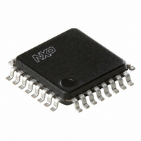
TDA8029HL/C207,118 NXP Semiconductors, TDA8029HL/C207,118 Datasheet - Page 10

TDA8029HL/C207,118
Manufacturer Part Number
TDA8029HL/C207,118
Description
IC SMART CARD READER 32-LQFP
Manufacturer
NXP Semiconductors
Datasheet
1.TDA8029HLC207118.pdf
(59 pages)
Specifications of TDA8029HL/C207,118
Package / Case
32-LQFP
Controller Type
Smart Card Reader Interface
Interface
Serial
Voltage - Supply
2.7 V ~ 6 V
Current - Supply
250mA
Operating Temperature
-40°C ~ 90°C
Mounting Type
Surface Mount
Maximum Operating Temperature
+ 90 C
Minimum Operating Temperature
- 40 C
Mounting Style
SMD/SMT
Lead Free Status / RoHS Status
Lead free / RoHS Compliant
Lead Free Status / RoHS Status
Lead free / RoHS Compliant, Lead free / RoHS Compliant
Other names
568-2233-2
935274733118
TDA8029HL07BD-T
935274733118
TDA8029HL07BD-T
Available stocks
Company
Part Number
Manufacturer
Quantity
Price
Company:
Part Number:
TDA8029HL/C207,118
Manufacturer:
NXP Semiconductors
Quantity:
10 000
Part Number:
TDA8029HL/C207,118
Manufacturer:
NXP/恩智浦
Quantity:
20 000
Philips Semiconductors
9397 750 14145
Product data sheet
8.1.2 Oscillator characteristics
8.1.3 Reset
8.1.4 Low power modes
Port 2
Port 3
XTAL1 and XTAL2 are the input and output, respectively, of an inverting amplifier. The pins
can be configured for use as an on-chip oscillator. To drive the device from an external
clock source, XTAL1 should be driven while XTAL2 is left unconnected. There are no
requirements on the duty cycle of the external clock signal, because the input to the
internal clock circuitry is through a divide-by-two flip-flop. However, minimum and
maximum HIGH and LOW times specified must be observed.
The microcontroller is reset when the TDA8029 is reset, as described in
This section describes the low power modes of the microcontroller. Please refer to
Section 8.15
•
•
•
•
•
•
•
•
•
•
pulled LOW will source current because of the internal pull-ups. Port 1 also
receives the low-order address byte during program memory verification.
Alternate functions for port 1 include:
T2 (P1.0): timer/counter 2 external count input/clock out (see programmable
clock out)
T2EX (P1.1): timer/counter 2 reload/capture/direction control.
(P2.7 to P2.0): Port 2 is an 8-bit bidirectional I/O port with internal pull-ups.
Port 2 pins that have logic 1s written to them are pulled HIGH by the internal
pull-ups and can be used as inputs. As inputs, port 2 pins that are externally
being pulled LOW will source current because of the internal pull-ups. Port 2
emits the high-order address byte during fetches from external program
memory and during accesses to external data memory that use 16-bit
addresses (MOVX @DPTR). In this application, it uses strong internal
pull-ups when emitting logic 1s. During access to external data memory that
use 8-bit addresses (MOV @Ri), port 2 emits the contents of the P2 special
function register. Some port 2 pins receive the high order address bits during
EPROM programming and verification.
(P3.7 to P3.3, P3.1 and P3.0): Port 3 is a 7-bit bidirectional I/O port with
internal pull-ups. Port 3 pins that have logic 1s written to them are pulled
HIGH by the internal pull-ups and can be used as inputs. As inputs, port 3
pins that are externally being pulled LOW will source current because of the
pull-ups. Port 3 also serves the special features of the 80C51 family, as listed:
RxD (P3.0): serial input port
TxD (P3.1): serial output port
INT0 (P3.2): external interrupt 0 (pin INT0_N)
INT1 (P3.3): external interrupt 1 (pin INT1_N)
T0 (P3.4): timer 0 external input
T1 (P3.5): timer 1external input
WR (P3.6): external data memory write strobe
RD (P3.7): external data memory read strobe.
for additional information of the TDA8029 power reduction modes.
Rev. 03 — 22 February 2005
Low power single card reader
© Koninklijke Philips Electronics N.V. 2005. All rights reserved.
TDA8029
Section
8.11.
10 of 59


