FDC37C665GT-MS SMSC, FDC37C665GT-MS Datasheet - Page 126
FDC37C665GT-MS
Manufacturer Part Number
FDC37C665GT-MS
Description
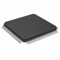
IC CTRLR SUPER I/O MULTI 100-QFP
Manufacturer
SMSC
Datasheet
1.FDC37C665GT-MS.pdf
(152 pages)
Specifications of FDC37C665GT-MS
Controller Type
I/O Controller
Interface
ISA Host
Voltage - Supply
4.5 V ~ 5.5 V
Current - Supply
35mA
Operating Temperature
0°C ~ 70°C
Mounting Type
Surface Mount
Package / Case
100-QFP
Lead Free Status / RoHS Status
Lead free / RoHS Compliant
Other names
638-1007
Available stocks
Company
Part Number
Manufacturer
Quantity
Price
Company:

Part Number:
FDC37C665GT-MS
Manufacturer:
Microchip Technology
Quantity:
10 000


CR5
This register can only be accessed when the
FDC is in the Configuration Mode and the
BIT NO.
4,3
0
1
2
5
6
7
1F0-1F7, 3F6,3F7
170-177, 376,377
ADDRESS
3F0-3F7
370-377
FDC Secondary
IDE Secondary
FDC DMA Mode
DenSel
swap drv 0,1
EXTx4
DS3
Table 53 - CR5- Floppy Disk and IDE Extended Setup Register
BIT NAME
A low level on this bit selects the primary address for the FDC
interface (Default). A high level on this bit selects the secondary
address space.
A low level on this bit selects the primary address for the IDE
interface (Default). A high level on this bit selects the secondary
address space.
0=(default) Burst mode is enabled for the FDC FIFO execution
phase data transfers. 1=Non-Burst mode enabled. The FDRQ
and FIRQ pins are strobed once for each byte transferred while
the FIFO is enabled.
A high level on this bit, swaps drives and motor sel 0 and 1 of the
FDC. A low level on this bit does not (Default).
External 4 drive support: 0=Internal 4 drive decoder (default).
1=External 4 drive decoder (External 2 to 4 decoder required).
Set to 0 (default) - Pin 98 is DS2 if ECP is not enabled by the
configuration or PDIR if ECP is enabled.
Set to 1 - Pin 98 is DS3 regardless of the parallel port mode.
Bit 4
0
0
1
1
BLOCK NAME
Floppy Disk
Floppy Disk
Bit 3
0
1
0
1
IDE
IDE
126
Densel output
Normal (Default)
Reserved
1
0
CSR has been initialized to 05H. The default
value after power up is 00H.
DESCRIPTION
Primary address
Secondary address
Primary address
Secondary address
NOTES
Related parts for FDC37C665GT-MS
Image
Part Number
Description
Manufacturer
Datasheet
Request
R

Part Number:
Description:
FAST ETHERNET PHYSICAL LAYER DEVICE
Manufacturer:
SMSC Corporation
Datasheet:
Part Number:
Description:
357-036-542-201 CARDEDGE 36POS DL .156 BLK LOPRO
Manufacturer:
SMSC Corporation
Datasheet:
Part Number:
Description:
357-036-542-201 CARDEDGE 36POS DL .156 BLK LOPRO
Manufacturer:
SMSC Corporation
Datasheet:
Part Number:
Description:
357-036-542-201 CARDEDGE 36POS DL .156 BLK LOPRO
Manufacturer:
SMSC Corporation
Datasheet:
Part Number:
Description:
4-PORT USB2.0 HUB CONTROLLER
Manufacturer:
SMSC Corporation
Datasheet:
Part Number:
Description:
Manufacturer:
SMSC Corporation
Datasheet:
Part Number:
Description:
Manufacturer:
SMSC Corporation
Datasheet:
Part Number:
Description:
FDC37C672ENHANCED SUPER I/O CONTROLLER WITH FAST IR
Manufacturer:
SMSC Corporation
Datasheet:
Part Number:
Description:
COM90C66LJPARCNET Controller/Transceiver with AT Interface and On-Chip RAM
Manufacturer:
SMSC Corporation
Datasheet:
Part Number:
Description:
Manufacturer:
SMSC Corporation
Datasheet:
Part Number:
Description:
Manufacturer:
SMSC Corporation
Datasheet:
Part Number:
Description:
Manufacturer:
SMSC Corporation
Datasheet:
Part Number:
Description:
Manufacturer:
SMSC Corporation
Datasheet: