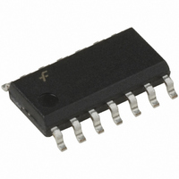
FIN1019M Fairchild Semiconductor, FIN1019M Datasheet - Page 2

FIN1019M
Manufacturer Part Number
FIN1019M
Description
IC DRVR/RCVR 3.3V HS LVDS 14SOIC
Manufacturer
Fairchild Semiconductor
Type
Line Transceiverr
Datasheet
1.FIN1019MX.pdf
(14 pages)
Specifications of FIN1019M
Number Of Drivers/receivers
1/1
Protocol
LVDS
Voltage - Supply
3 V ~ 3.6 V
Mounting Type
Surface Mount
Package / Case
14-SOIC (3.9mm Width), 14-SOL
Logic Family
FIN10
Logic Type
High Speed Differential Driver and Receiver
Supply Voltage (max)
3.6 V
Supply Voltage (min)
3 V
Maximum Operating Temperature
+ 85 C
Mounting Style
SMD/SMT
Data Rate
400 Mbps
Minimum Operating Temperature
- 40 C
Number Of Lines (input / Output)
1 / 1
Propagation Delay Time
2.5 ns
Supply Current
12.5 mA
Lead Free Status / RoHS Status
Lead free / RoHS Compliant
Other names
FIN1019M_NL
FIN1019M_NL
FIN1019M_NL
Available stocks
Company
Part Number
Manufacturer
Quantity
Price
Company:
Part Number:
FIN1019MX
Manufacturer:
Fairchild Semiconductor
Quantity:
26 058
Company:
Part Number:
FIN1019MX
Manufacturer:
FSC
Quantity:
8 920
Part Number:
FIN1019MX
Manufacturer:
FAIRCHILD/仙童
Quantity:
20 000
www.fairchildsemi.com
LVDS Differential Driver Characteristics
V
V
I
I
I
LVTTL Driver Characteristics
V
V
I
LVDS Receiver Characteristics
V
V
I
I
LVTTL Driver and Control Signals Characteristics
V
V
I
I
V
OZD
OFF
OS
OZ
IN
I(OFF)
IN
I(OFF)
Absolute Maximum Ratings
DC Electrical Characteristics
Over supply voltage and operating temperature ranges, unless otherwise specified
Supply Voltage (V
LVTTL DC Input Voltage (D
LVDS DC Input Voltage (R
LVTTL DC Output Voltage (R
LVDS DC Output Voltage (D
LVDS Driver Short Circuit Current (I
LVTTL DC Output Current (I
Storage Temperature Range (T
Max Junction Temperature (T
Lead Temperature (T
ESD (Human Body Model)
ESD (Machine Model)
OD
V
OS
V
OH
OL
TH
TL
IH
IL
IK
Symbol
OD
OS
(Soldering, 10 seconds)
Output Differential Voltage
V
Differential LOW-to-HIGH
Offset Voltage
Offset Magnitude Change from
Differential LOW-to-HIGH
Disabled Output Leakage Current
Power Off Output Current
Short Circuit Output Current
Output HIGH Voltage
Output LOW Voltage
Disabled Output Leakage Current
Differential Input Threshold HIGH
Differential Input Threshold LOW
Input Current
Power-OFF Input Current
Input HIGH Voltage
Input LOW Voltage
Input Current
Power-OFF Input Current
Input Clamp Voltage
OD
Magnitude Change from
CC
)
L
)
Parameter
IN
IN
O
OUT
, DE, RE)
OUT
, R
)
J
)
STG
IN
)
, D
)
)
OSD
OUT
)
)
65 C to 150 C
R
V
V
V
V
I
See Figure 6 and Table 1
I
V
I
See Figure 6 and Table 1
I
V
V
See Figure 6 and Table 1
See Figure 6 and Table 1
V
V
V
V
I
OH
OH
OL
OL
IK
(Note 1)
0.5V to 4.6V
L
OUT
CC
OUT
OD
ID
ID
OUT
IN
CC
IN
CC
0.5V to 4.7V
0.5V to 4.7V
0.5V to 6V
0.5V to 6V
Continuous
100 , See Figure 1
100 A, RE
400 mV, V
0V or V
0V or V
18 mA
0V, V
0V, DE
8 mA, RE
0V, V
0V, V
100 A, RE
8 mA, RE
400 mV, V
V
0V, DE
V
16 mA
6500V
CC
CC
150 C
260 C
300V
OUT
IN
IN
or GND, DE
or GND, RE
Test Conditions
CC
CC
V
IC
0V or 3.6V
0V or 3.6V
V
IC
CC
2
0V or 3.6V
CC
0V, V
0V, V
0V, V
Recommended Operating
Conditions
Note 1: The “Absolute Maximum Ratings”: are those values beyond which
damage to the device may occur. The databook specifications should be
met, without exception, to ensure that the system design is reliable over its
power supply, temperature and output/input loading variables. Fairchild
does not recommend operation of circuits outside databook specification.
1.2V, see Figure 6
Supply Voltage (V
Input Voltage (V
Magnitude of Differential Voltage
Common-Mode Input Voltage (V
Operating Temperature (T
0V,
1.2V, see Figure 6
(|V
ID
ID
ID
ID
0V
V
CC
400 mV
|)
400 mV
400 mV
IN
CC
)
)
V
CC
1.125
GND
Min
250
2.4
2.0
100
1.5
A
0.2
)
(Note 2)
IC
1.25
)
Typ
350
1.375
Max
V
450
100
100 mV to V
0.05V to 2.35V
0.2
0.5
0.8
25
25
40 C to 85 C
20
20
20
20
20
CC
20
20
8
8
3.0V to 3.6V
0 to V
Units
mV
mV
mV
mA
mV
mV
V
V
V
V
V
V
A
A
A
A
A
A
A
CC
CC


