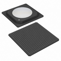
DS26519GN+ Maxim Integrated Products, DS26519GN+ Datasheet - Page 307

DS26519GN+
Manufacturer Part Number
DS26519GN+
Description
IC TXRX T1/E1/J1 16PRT 484-HSBGA
Manufacturer
Maxim Integrated Products
Type
Transceiverr
Datasheet
1.DS26519GN.pdf
(310 pages)
Specifications of DS26519GN+
Number Of Drivers/receivers
16/16
Protocol
Ethernet
Voltage - Supply
3.135 V ~ 3.465 V
Mounting Type
Surface Mount
Package / Case
484-BGA Exposed Pad, 484-eBGA, 484-HBGA
Lead Free Status / RoHS Status
Lead free / RoHS Compliant
- Current page: 307 of 310
- Download datasheet (9Mb)
14.3
Table 14-2. ID Code Structure
14.4
IEEE 1149.1 requires a minimum of two test registers: the Bypass Register and the Boundary Scan Register. An
optional test register, the Identification Register, has been included with the DS26519 design. The Identification
Register is used in conjunction with the IDCODE instruction and the Test-Logic-Reset state of the TAP controller.
14.4.1 Boundary Scan Register
This register contains both a shift register path and a latched parallel output for all control cells and digital I/O cells,
and is n bits in length.
14.4.2 Bypass Register
This register is a single one-bit shift register used in conjunction with the BYPASS, CLAMP, and HIGHZ
instructions, providing a short path between JTDI and JTDO.
14.4.3 Identification Register
The Identification Register contains a 32-bit shift register and a 32-bit latched parallel output. This register is
selected during the IDCODE instruction and when the TAP controller is in the Test-Logic-Reset state.
DS26519
DS26518
DEVICE
JTAG ID Codes
Test Registers
Consult factory
Consult factory
REVISION
ID[31:28]
0000000010001011
0000000010001010
DEVICE CODE
ID[27:12]
307 of 310
MANUFACTURER’S CODE
00010100001
00010100001
ID[11:1]
DS26519 16-Port T1/E1/J1 Transceiver
REQUIRED
ID[0]
1
1
Related parts for DS26519GN+
Image
Part Number
Description
Manufacturer
Datasheet
Request
R

Part Number:
Description:
Ds26519 16-port T1/e1/j1 Transceiver
Manufacturer:
Maxim Integrated Products, Inc.
Datasheet:

Part Number:
Description:
power light source LUXEON® Collimator
Manufacturer:
LUMILEDS [Lumileds Lighting Company]
Datasheet:

Part Number:
Description:
MAX7528KCWPMaxim Integrated Products [CMOS Dual 8-Bit Buffered Multiplying DACs]
Manufacturer:
Maxim Integrated Products
Datasheet:

Part Number:
Description:
Single +5V, fully integrated, 1.25Gbps laser diode driver.
Manufacturer:
Maxim Integrated Products
Datasheet:

Part Number:
Description:
Single +5V, fully integrated, 155Mbps laser diode driver.
Manufacturer:
Maxim Integrated Products
Datasheet:

Part Number:
Description:
VRD11/VRD10, K8 Rev F 2/3/4-Phase PWM Controllers with Integrated Dual MOSFET Drivers
Manufacturer:
Maxim Integrated Products
Datasheet:

Part Number:
Description:
Highly Integrated Level 2 SMBus Battery Chargers
Manufacturer:
Maxim Integrated Products
Datasheet:

Part Number:
Description:
Current Monitor and Accumulator with Integrated Sense Resistor; ; Temperature Range: -40°C to +85°C
Manufacturer:
Maxim Integrated Products

Part Number:
Description:
TSSOP 14/A°/RS-485 Transceivers with Integrated 100O/120O Termination Resis
Manufacturer:
Maxim Integrated Products

Part Number:
Description:
TSSOP 14/A°/RS-485 Transceivers with Integrated 100O/120O Termination Resis
Manufacturer:
Maxim Integrated Products

Part Number:
Description:
QFN 16/A°/AC-DC and DC-DC Peak-Current-Mode Converters with Integrated Step
Manufacturer:
Maxim Integrated Products

Part Number:
Description:
TDFN/A/65V, 1A, 600KHZ, SYNCHRONOUS STEP-DOWN REGULATOR WITH INTEGRATED SWI
Manufacturer:
Maxim Integrated Products

Part Number:
Description:
Integrated Temperature Controller f
Manufacturer:
Maxim Integrated Products

Part Number:
Description:
SOT23-6/I°/45MHz to 650MHz, Integrated IF VCOs with Differential Output
Manufacturer:
Maxim Integrated Products


