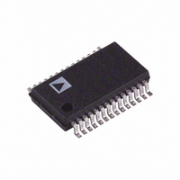
AD1896AYRSZ Analog Devices Inc, AD1896AYRSZ Datasheet - Page 22

AD1896AYRSZ
Manufacturer Part Number
AD1896AYRSZ
Description
IC CONV SAMPLE RATE ASYNC 28SSOP
Manufacturer
Analog Devices Inc
Type
Sample Rate Converterr
Datasheet
1.AD1896AYRSZ.pdf
(28 pages)
Specifications of AD1896AYRSZ
Applications
Automotive Audio, processing, receivers
Voltage - Supply, Digital
3.13 V ~ 3.46 V
Mounting Type
Surface Mount
Package / Case
28-SSOP
Audio Control Type
Sample Rate Converter
Output Power
132mW
Supply Voltage Range
3.135V To 3.465V, 3.135V To 5.5V
Operating Temperature Range
-40°C To +105°C
Audio Ic Case Style
SSOP
Lead Free Status / RoHS Status
Lead free / RoHS Compliant
Voltage - Supply, Analog
-
Lead Free Status / RoHS Status
Lead free / RoHS Compliant, Lead free / RoHS Compliant
Available stocks
Company
Part Number
Manufacturer
Quantity
Price
Company:
Part Number:
AD1896AYRSZRL
Manufacturer:
CYPRESS
Quantity:
92
AD1896
There are, of course, maximum and minimum operating fre-
quencies for the AD1896 master clock. The maximum master
clock frequency at which the AD1896 is guaranteed to operate is
30 MHz. A frequency of 30 MHz is more than sufficient to
sample rate convert sampling frequencies of 192 kHz + 12%.
The minimum required frequency for the master clock generation
for the AD1896 depends upon the input and output sample
rates. The master clock has to be at least 138 times greater than
the maximum input or output sample rate.
Serial Data Ports—Data Format
The serial data input port mode is set by the logic levels on the
SMODE_IN_0/SMODE_IN_1/SMODE_IN_2 pins. The serial
data input port modes available are left justified, I
justified (RJ), 16, 18, 20, or 24 bits as defined in Table I.
Figure 9a. Fundamental-Mode Circuit Configuration
Figure 9b. Third-Overtone Circuit Configuration
AD1896
MCLK_I
AD1896
MCLK_I
C1
C1
MCLK_O
R
C2
MCLK_O
C2
R
1nF
L1
2
S, and right
–22–
2
0
0
0
0
1
1
1
1
The serial data output port mode is set by the logic levels on the
SMODE_OUT_0/SMODE_OUT_1 and WLNGTH_OUT_0/
WLNGTH_OUT_1 pins. The serial mode can be changed to
left justified, I
lowing table. The output word width can be set by using the
WLNGTH_OUT_0/WLNGTH_OUT_1 pins as shown in
Table III. When the output word width is less than 24 bits, dither
is added to the truncated bits. The right justified serial data out
mode assumes 64 SCLK_O cycles per frame, divided evenly for
left and right. Please note that 8 bits of each 32-bit subframe are
used for transmitting matched-phase mode data. Please refer to
Figure 14. The AD1896 also supports 16-bit, 32-clock packed
input and output serial data in LJ and I
SMODE_OUT_[0:1]
1
0
0
1
1
WLNGTH_OUT_[0:1]
1
0
0
1
1
The following timing diagrams show the serial mode formats.
SMODE_IN_[0:2]
1
0
0
1
1
0
0
1
1
Table II. Serial Data Output Port Mode
Table I. Serial Data Input Port Mode
2
S, right justified, or TDM as defined in the fol-
0
0
1
0
1
0
0
1
0
1
Table III. Word Width
0
0
1
0
1
0
1
0
1
Interface Format
Left Justified (LJ)
I
TDM Mode
Right Justified (RJ)
Word Width
24 Bits
20 Bits
18 Bits
16 Bits
2
S
Interface Format
Left Justified
I
Undefined
Undefined
Right Justified, 16 Bits
Right Justified, 18 Bits
Right Justified, 20 Bits
Right Justified, 24 Bits
2
S
2
S format.
REV. A


