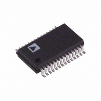
AD1896AYRSZ Analog Devices Inc, AD1896AYRSZ Datasheet - Page 25

AD1896AYRSZ
Manufacturer Part Number
AD1896AYRSZ
Description
IC CONV SAMPLE RATE ASYNC 28SSOP
Manufacturer
Analog Devices Inc
Type
Sample Rate Converterr
Datasheet
1.AD1896AYRSZ.pdf
(28 pages)
Specifications of AD1896AYRSZ
Applications
Automotive Audio, processing, receivers
Voltage - Supply, Digital
3.13 V ~ 3.46 V
Mounting Type
Surface Mount
Package / Case
28-SSOP
Audio Control Type
Sample Rate Converter
Output Power
132mW
Supply Voltage Range
3.135V To 3.465V, 3.135V To 5.5V
Operating Temperature Range
-40°C To +105°C
Audio Ic Case Style
SSOP
Lead Free Status / RoHS Status
Lead free / RoHS Compliant
Voltage - Supply, Analog
-
Lead Free Status / RoHS Status
Lead free / RoHS Compliant, Lead free / RoHS Compliant
Available stocks
Company
Part Number
Manufacturer
Quantity
Price
Company:
Part Number:
AD1896AYRSZRL
Manufacturer:
CYPRESS
Quantity:
92
Matched-Phase Mode
The matched-phase mode is the mode discussed in the Theory of
Operation section that eliminates the phase mismatch between
multiple AD1896s. The master AD1896 device transmits
its f
AD1896’s TDM_IN pins. The slave AD1896s receive the
transmitted f
f
ratio. The master device can have both its serial ports in slave
mode as depicted or either one in master mode. The slave
AD1896s must have their MMODE_2, MMODE_1, and
MMODE_0 pins set to 100, respectively. LRCLK_I and
LRCLK_O may be asynchronous with respect to each other in
this mode. Another requirement of the matched-phase mode is
that there must be 32 SCLK_O cycles per subframe. The
AD1896 will support the matched-phase mode for all serial
output data formats, left justified, I
TDM. In the case of TDM, the AD1896 shown in the TDM
mode operation figure with its TDM_IN tied to ground would be
REV. A
S_IN
S_OUT
ratio instead of their own internally derived f
/f
S_IN
S_OUT
ratio through the SDATA_O pin to the slave
MATCHED-PHASE
AUDIO DATA LEFT CHANNEL, 24 BITS
DATA, 8 BITS
/f
S_IN
Figure 14a. Matched-Phase Data Transmission (Left-Justified, I
ratio and use the transmitted f
Figure 14b. Matched-Phase Data Transmission (Right-Justified Mode)
2
S, right justified, and
AUDIO DATA LEFT CHANNEL,
16 BITS – 24 BITS
S_OUT
MATCHED-PHASE
DATA, 8 BITS
S_OUT
/f
S_IN
/
–25–
MATCHED-PHASE
configured as the master, while the rest of the AD1896s in the
chain would be configured as slaves with their MMODE_2,
MMODE_1, and MMODE_0 pins set to 100, respectively.
Please note that in the left-justified, I
the lower eight bits of each channel subframe are used to
transmit the matched-phase data. In right-justified mode, the
upper eight bits are used to transmit the matched-phase data.
This is shown in Figures 14a and 14b.
Bypass Mode
When the BYPASS pin is asserted high, the input data bypasses
the sample rate converter and is sent directly to the serial output
port. Dithering of the output data when the word length is set
to less than 24 bits is disabled. This mode is ideal when the
input and output sample rates are the same and LRCLK_I and
LRCLK_O are synchronous with respect to each other. This
mode can also be used for passing through non-AUDIO data
since no processing is performed on the input data in this mode.
AUDIO DATA RIGHT CHANNEL, 24 BITS
DATA, 8 BITS
AUDIO DATA RIGHT CHANNEL,
2
S, and TDM Mode)
16 BITS – 24 BITS
MATCHED-PHASE
DATA, 8 BITS
2
S, and TDM modes,
AD1896


