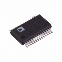
AD1896AYRSZ Analog Devices Inc, AD1896AYRSZ Datasheet - Page 3

AD1896AYRSZ
Manufacturer Part Number
AD1896AYRSZ
Description
IC CONV SAMPLE RATE ASYNC 28SSOP
Manufacturer
Analog Devices Inc
Type
Sample Rate Converterr
Datasheet
1.AD1896AYRSZ.pdf
(28 pages)
Specifications of AD1896AYRSZ
Applications
Automotive Audio, processing, receivers
Voltage - Supply, Digital
3.13 V ~ 3.46 V
Mounting Type
Surface Mount
Package / Case
28-SSOP
Audio Control Type
Sample Rate Converter
Output Power
132mW
Supply Voltage Range
3.135V To 3.465V, 3.135V To 5.5V
Operating Temperature Range
-40°C To +105°C
Audio Ic Case Style
SSOP
Lead Free Status / RoHS Status
Lead free / RoHS Compliant
Voltage - Supply, Analog
-
Lead Free Status / RoHS Status
Lead free / RoHS Compliant, Lead free / RoHS Compliant
Available stocks
Company
Part Number
Manufacturer
Quantity
Price
Company:
Part Number:
AD1896AYRSZRL
Manufacturer:
CYPRESS
Quantity:
92
REV. A
DIGITAL TIMING (–40 C < T
Parameter
t
f
t
t
Input Serial Port Timing
t
t
t
t
t
Propagation Delay from MCLK_I Rising Edge to SCLK_I Rising Edge
(Serial Input Port MASTER)
Propagation Delay from MCLK_I Rising Edge to LRCLK_I Rising Edge
(Serial Input Port MASTER)
Output Serial Port Timing
t
t
t
t
t
t
t
t
t
Propagation Delay from MCLK_I Rising Edge to SCLK_O Rising Edge
(Serial Output Port MASTER)
Propagation Delay from MCLK_I Rising Edge to LRCLK_O Rising Edge
(Serial Output Port MASTER)
NOTES
1
2
3
Specifications subject to change without notice.
MCLKI
MCLK
MPWH
MPWL
LRIS
SIH
SIL
DIS
DIH
TDMS
TDMH
DOPD
DOH
LROS
LROH
SOH
SOL
RSTL
Refer to Timing Diagrams section.
The maximum possible sample rate is: FS
f
MCLK
of up to 34 MHz is possible under the following conditions: 0∞C < T
1
MCLK_I Period
MCLK_I Frequency
MCLK_I Pulsewidth High
MCLK_I Pulsewidth Low
LRCLK_I Setup to SCLK_I
SCLK_I Pulsewidth High
SCLK_I Pulsewidth Low
SDATA_I Setup to SCLK_I Rising Edge
SDATA_I Hold from SCLK_I Rising Edge
TDM_IN Setup to SCLK_O Falling Edge
TDM_IN Hold from SCLK_O Falling Edge
SDATA_O Propagation Delay from SCLK_O, LRCLK_O
SDATA_O Hold from SCLK_O
LRCLK_O Setup to SCLK_O (TDM Mode Only)
LRCLK_O Hold from SCLK_O (TDM Mode Only)
SCLK_O Pulsewidth High
SCLK_O Pulsewidth Low
RESET Pulsewidth Low
A
< +105 C, VDD_CORE = 3.3 V
MAX
= f
MCLK
/138.
A
< 70∞C, 45/55 or better MCLK_I duty cycle.
–3–
5%, VDD_IO = 5.0 V
Min
3
33.3
9
12
8
8
8
8
3
3
3
3
5
10
5
200
10%)
Typ
Max
30.0
12
12
20
12
12
2, 3
AD1896
Unit
ns
MHz
ns
ns
ns
ns
ns
ns
ns
ns
ns
ns
ns
ns
ns
ns
ns
ns
ns
ns
ns
ns


