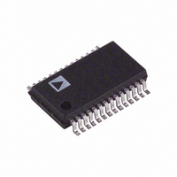
AD1895AYRSRL Analog Devices Inc, AD1895AYRSRL Datasheet - Page 17

AD1895AYRSRL
Manufacturer Part Number
AD1895AYRSRL
Description
IC SAMP-RATEHP/CONV 24BIT 28SSOP
Manufacturer
Analog Devices Inc
Type
Sample Rate Converterr
Datasheet
1.AD1895AYRSZ.pdf
(24 pages)
Specifications of AD1895AYRSRL
Rohs Status
RoHS non-compliant
Applications
Automotive Audio, receivers, set-top boxes
Voltage - Supply, Digital
3.13 V ~ 3.46 V
Mounting Type
Surface Mount
Package / Case
28-SSOP
For Use With
EVAL-AD1895EB - BOARD EVAL FOR AD1895
Voltage - Supply, Analog
-
Lead Free Status / RoHS Status
Not Compliant
Available stocks
Company
Part Number
Manufacturer
Quantity
Price
Company:
Part Number:
AD1895AYRSRL
Manufacturer:
MOTOROLA
Quantity:
4 900
Part Number:
AD1895AYRSRL
Manufacturer:
ADI/亚德诺
Quantity:
20 000
HARDWARE MODEL
The output rate of the low-pass filter of Figure 5 would be the
interpolation rate, 2
a rate of 201.3 GHz is clearly impractical, not to mention the
number of taps required to calculate each interpolated sample.
However, since interpolation by 2
samples between each f
the low-pass FIR filter are by zero. A further reduction can be
realized by the fact that since only one interpolated sample is
taken at the output at the f
needs to be performed per f
lutions. A 64-tap FIR filter for each f
to suppress the images caused by the interpolation.
The difficulty with the above approach is that the correct inter-
polated sample needs to be selected upon the arrival of f
Since there are 2
arrival of the f
of 1/201.3 GHz = 4.96 ps. Measuring the f
clock of 201.3 GHz frequency is clearly impossible; instead,
several coarse measurements of the f
and averaged over time.
Another difficulty with the above approach is the number of
coefficients required. Since there are 2
with a 64-tap FIR filter, there needs to be 2
cients for each tap, which requires a total of 2
reduce the number of coefficients in ROM, the AD1895 stores a
small subset of coefficients and performs a high order interpola-
tion between the stored coefficients. So far, the above approach
works for the case of f
the output sample rate, f
REV. B
IN
Figure 6. Frequency Domain of the Interpolation and
Resampling
f
S_IN
FREQUENCY DOMAIN OF SAMPLES AT
FREQUENCY DOMAIN OF THE INTERPOLATION
FREQUENCY DOMAIN OF
FREQUENCY DOMAIN AFTER
RESAMPLING
SIN(X)/X OF ZERO-ORDER HOLD
INTERPOLATE
S_OUT
BY N
20
possible convolutions per f
20
clock must be measured with an accuracy
S_OUT
× 192000 kHz = 201.3 GHz. Sampling at
S_IN
S_OUT
S_OUT
> f
sample, most of the multiplies in
f
LOW-PASS
S_OUT
S_OUT
, is less than the input sample
FILTER
S_IN
RESAMPLING
20
rate, only one convolution
. However, in the case when
period instead of 2
involves zero-stuffing 2
S_OUT
S_OUT
20
f
S_IN
2
possible convolutions
20
ZERO-ORDER
clock period are made
S_OUT
sample is sufficient
20
f
S_IN
HOLD
26
S_OUT
polyphase coeffi-
2
2
20
f
S_IN
20
coefficients. To
period with a
f
S_IN
f
period, the
S_IN
20
S_OUT
f
convo-
S_OUT
20
OUT
–1
.
–17–
rate, f
the convolution must be scaled. As the input sample rate rises
over the output sample rate, the antialiasing filter’s cutoff fre-
quency has to be lowered because the Nyquist frequency of the
output samples is less than the Nyquist frequency of the input
samples. To move the cutoff frequency of the antialiasing filter,
the coefficients are dynamically altered and the length of the
convolution is increased by a factor of f
nique is supported by the Fourier transform property that if f(t)
is F(ω), then f(k × t) is F(ω/k). Thus, the range of decimation is
simply limited by the size of the RAM.
THE SAMPLE RATE CONVERTER ARCHITECTURE
The architecture of the sample rate converter is shown in
Figure 7. The sample rate converter’s FIFO block adjusts the
left and right input samples and stores them for the FIR filter’s
convolution cycle. The f
the FIFO block and the ramp input to the digital servo loop. The
ROM stores the coefficients for the FIR filter convolution and
performs a high order interpolation between the stored coefficients.
The sample rate ratio block measures the sample rate for dynami-
cally altering the ROM coefficients and scaling of the FIR filter
length as well as the input data. The digital servo loop automatically
tracks the f
and ROM start addresses for the start of the FIR filter convolution.
The FIFO receives the left and right input data and adjusts the
amplitude of the data for both the soft muting of the sample rate
converter and the scaling of the input data by the sample rate
ratio before storing the samples in the RAM. The input data
is scaled by the sample rate ratio because as the FIR filter length
of the convolution increases, so does the amplitude of the convo-
lution output. To keep the output of the FIR filter from saturating,
the input data is scaled down by multiplying it by f
when f
muting and unmuting the AD1895.
The RAM in the FIFO is 512 words deep for both left and right
channels. A small offset of 16 is added to the write address
provided by the f
from ever overlapping the write address. The maximum deci-
mation rate can be calculated from the RAM word depth as
(512 – 16)/64 taps = 7.75 and a small offset.
Figure 7. Architecture of the Sample Rate Converter
RIGHT DATA IN
S_IN
LEFT DATA IN
COUNTER
S_OUT
f
S_IN
, the ROM starting address, input data, and length of
S_IN
f
S_OUT
< f
f
S_IN
and f
S_IN
S_IN
. The FIFO also scales the input data for
SAMPLE RATE RATIO
S_OUT
SAMPLE RATE
counter to prevent the RAM read pointer
SERVO LOOP
S_IN
DIGITAL
RATIO
FIFO
sample rates and provides the RAM
counter provides the write address to
EXTERNAL
RATIO
ROM A
ROM B
ROM C
ROM D
S_IN
FIR FILTER
/f
S_OUT
AD1895
L/R DATA OUT
HIGH
ORDER
INTERP
S_OUT
. This tech-
/f
S_IN


