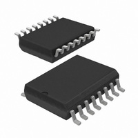
PCA9500D,112 NXP Semiconductors, PCA9500D,112 Datasheet - Page 24

PCA9500D,112
Manufacturer Part Number
PCA9500D,112
Description
IC I/O EXPANDER I2C 8B 16SOIC
Manufacturer
NXP Semiconductors
Datasheet
1.PCA9500BS118.pdf
(26 pages)
Specifications of PCA9500D,112
Interface
I²C, SMBus
Number Of I /o
8
Interrupt Output
No
Frequency - Clock
400kHz
Voltage - Supply
2.5 V ~ 3.6 V
Operating Temperature
-40°C ~ 85°C
Mounting Type
Surface Mount
Package / Case
16-SOIC (0.300", 7.5mm Width)
Includes
EEPROM, POR
Lead Free Status / RoHS Status
Lead free / RoHS Compliant
Other names
568-1024-5
935271533112
PCA9500D
935271533112
PCA9500D
NXP Semiconductors
16. Revision history
Table 11.
PCA9500_4
Product data sheet
Document ID
PCA9500_4
Modifications:
PCA9500_3
(9397 750 14134)
PCA9500_2
PCA9500_1
Revision history
Release date
20090415
20040930
20030627
20020927
•
•
•
•
•
•
•
•
•
•
•
The format of this data sheet has been redesigned to comply with the new identity
guidelines of NXP Semiconductors.
Legal texts have been adapted to the new company name where appropriate.
Table 3 “Pin
– added
– changed naming convention for pins I/On to “IOn”
Figure 7 “I/O Write mode
Figure 8 “I/O Read mode
– changed symbol “t
– changed symbol “t
Table 4 “Limiting
– changed symbol “V
– changed parameter for I
– changed symbol “P
– changed parameter for T
Table 5 “Static
– added reference to
Table 6 “Dynamic
– sub-section “I
– sub-section “Port timing”: changed symbol “t
– sub-section “Port timing”: changed symbol “t
– sub-section “Port timing”: changed symbol “t
– sub-section “Power-up timing”: changed symbol “t
– sub-section “Power-up timing”: changed symbol “t
– sub-section “Write cycle limits”: changed symbol “t
Figure 23 “Write cycle
added
updated soldering information
placed “operating” in Conditions column
width on bus” to “t
Section 15 “Abbreviations”
Table note [1]
description”:
Data sheet status
Product data sheet
Product data sheet
Product data
Product data
characteristics”:
2
values”:
C-bus timing”: changed symbol/parameter from “t
characteristics”:
Rev. 04 — 15 April 2009
SP
ph
ps
CC
O
timing”: changed symbol “t
Table note [1]
, pulse width of spikes that must be suppressed by the input filter”
” to “t
” to “t
” to “P/out”
and its reference at HVQFN16 pin 6
” to “V
(output)”: changed symbol “t
(input)”:
SS
amb
8-bit I
su(D)
h(D)
from “supply current” to “ground supply current”
DD
from “operating temperature” to “ambient temperature”;
”
”
”
2
C-bus and SMBus I/O port with 2-kbit EEPROM
at I
OL
in sub-section “I/O expander port”
Change notice
-
-
853-2369 30018
of 2003 Jun 11
853-2369 28875
of 2002 Sep 27
pv
ps
ph
WR
” to “t
” to “t
” to “t
” to “T
PUR
PUW
WR
pv
v(Q)
su(D)
h(D)
” to “t
” to “T
” to “t
” to “t
”
”
cy(W)
”
v(Q)
pu(R)
pu(W)
cy(W)
”
”
”
”
”
SW
, tolerable spike
PCA9500
© NXP B.V. 2009. All rights reserved.
Supersedes
PCA9500_3
PCA9500_2
PCA9500_1
-
24 of 26


