DS92LV16TVHG/NOPB National Semiconductor, DS92LV16TVHG/NOPB Datasheet - Page 18
DS92LV16TVHG/NOPB
Manufacturer Part Number
DS92LV16TVHG/NOPB
Description
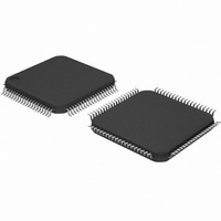
IC SERDES LVDS 16BIT BUS 80-LQFP
Manufacturer
National Semiconductor
Datasheet
1.DS92LV16TVHGNOPB.pdf
(19 pages)
Specifications of DS92LV16TVHG/NOPB
Function
Serializer/Deserializer
Data Rate
2.56Gbps
Input Type
LVTTL/LVCMOS
Output Type
LVTTL, LVCMOS
Number Of Inputs
1
Number Of Outputs
16
Voltage - Supply
3.15 V ~ 3.45 V
Operating Temperature
-40°C ~ 85°C
Mounting Type
Surface Mount
Package / Case
80-LQFP
No. Of Inputs
16
No. Of Outputs
16
Supply Voltage Range
3.15V To 3.45V
Driver Case Style
QFP
No. Of Pins
80
Msl
MSL 3 - 168 Hours
Filter Terminals
SMD
Rohs Compliant
Yes
Data Rate Max
1280Mbps
For Use With
BLVDS16EVK - BOARD EVAL FOR DS92LV16
Lead Free Status / RoHS Status
Lead free / RoHS Compliant
Other names
*DS92LV16TVHG
*DS92LV16TVHG/NOPB
DS92LV16TVHG
*DS92LV16TVHG/NOPB
DS92LV16TVHG
Available stocks
Company
Part Number
Manufacturer
Quantity
Price
Company:

Part Number:
DS92LV16TVHG/NOPB
Manufacturer:
NSC
Quantity:
251
Company:
Part Number:
DS92LV16TVHG/NOPB
Manufacturer:
Texas Instruments
Quantity:
10 000


www.national.com
Pin Descriptions
21, 22, 23, 24, 25, 26,
27, 28, 33, 34, 35, 36,
41, 44, 51, 52, 59, 60,
45, 46, 47, 48, 54, 55,
56, 57, 64, 65, 66, 67,
Note 8: Input defaults to ’low’ state when left open due to internal pull-device.
43, 50, 53, 58, 62, 69
Pin #
37, 38, 39, 40
70, 71, 72, 73
5, 10, 11, 15
61, 68, 80
6,9,12,16
29,32
30,31
74,76
75,77
13
14
17
18
19
20
42
49
63
78
79
1
2
3
4
7
8
ROUT (0:15)
LOCAL_LE
DIN (0:15)
Pin Name
CONFIG1
CONFIG2
RPWDN*
TPWDN*
REFCLK
LINE_LE
LOCK*
DGND
AGND
SYNC
PGND
PVDD
DVDD
PGND
PVDD
AVDD
RCLK
TCLK
RIN+
REN
DO+
DEN
RIN-
DO-
CMOS, O Receiver Outputs.
CMOS, O Recovered Clock. Parallel data rate clock recovered from
CMOS, O LOCK* indicates the status of the receiver PLL. LOCK = H -
LVDS, O Transmitter LVDS True Output
LVDS, O Transmitter LVDS Inverting Output
CMOS, I
CMOS, I
CMOS, I
CMOS, I
CMOS, I
CMOS, I
CMOS, I
CMOS, I
CMOS, I
CMOS, I
LVDS, I
LVDS, I
I/O
RPWDN* = Low will put the Receiver in low power, stand-by,
mode. Note: The Receiver PLL will lose lock.(Note 8)
REN = Low will disable the Receiver outputs. Receiver PLL
remains locked. (See LOCK pin description)(Note 8)
Configuration pin - strap or tie this pin to High with pull-up resistor.
No-connect or Low reserved for future use.
Frequency reference clock input for the receiver.
Analog Voltage Supply
Analog Ground
Receiver LVDS True Input
Receiver LVDS Inverting Input
Transmitter reference clock. Used to strobe data at the DIN Inputs
and to drive the transmitter PLL. See TCLK Timing Requirements.
Configuration pin - strap or tie this pin to High with pull-up resistor.
No-connect or Low reserved for future use.
DEN = Low will disable the Transmitter outputs. The transmitter
PLL will remain locked.(Note 8)
SYNC = High will cause the transmitter to ignore the data inputs
and send SYNC patterns to provide a locking reference to
receiver(s). See Functional Description.(Note 8)
Transmitter data inputs.(Note 8)
PLL Ground.
PLL Voltage supply.
Digital Ground.
TPWDN* = Low will put the Transmitter in low power, stand-by
mode. Note: The transmitter PLL will lose lock.(Note 8)
Digital Voltage Supplies.
embedded clock. Used to strobe ROUT (0:15). LVCMOS Level
output.
receiver PLL is unlocked, LOCK = L - receiver PLL is locked.
PLL Grounds.
PLL Voltage Supplies.
LINE_LE = High enables the receiver loopback mode. Data
received at the RIN+/- inputs is fed back through the DO+/-
outputs.(Note 8)
LOCAL_LE = High enables the transmitter loopback mode. Date
received at the DIN inputs is fed back through the ROUT
outputs.(Note 8)
18
Description
Related parts for DS92LV16TVHG/NOPB
Image
Part Number
Description
Manufacturer
Datasheet
Request
R

Part Number:
Description:
National Semiconductor [8-Bit D/A Converter]
Manufacturer:
National Semiconductor
Datasheet:
Part Number:
Description:
National Semiconductor [Media Coprocessor]
Manufacturer:
National Semiconductor
Datasheet:
Part Number:
Description:
Digitally Controlled Tone and Volume Circuit with Stereo Audio Power Amplifier, Microphone Preamp Stage and National 3D Sound
Manufacturer:
National Semiconductor
Datasheet:
Part Number:
Description:
Digitally Controlled Tone and Volume Circuit with Stereo Audio Power Amplifier, Microphone Preamp Stage and National 3D Sound
Manufacturer:
National Semiconductor
Datasheet:
Part Number:
Description:
AC97 Rev 2 Codec with Sample Rate Conversion and National 3D Sound
Manufacturer:
National Semiconductor
Part Number:
Description:
Manufacturer:
National Semiconductor
Datasheet:
Part Number:
Description:
Manufacturer:
National Semiconductor
Datasheet:
Part Number:
Description:
General Purpose, Low Voltage, Low Power, Rail-to-Rail Output Operational Amplifiers
Manufacturer:
National Semiconductor
Datasheet:
Part Number:
Description:
8-bit 20 MSPS flash A/D converter.
Manufacturer:
National Semiconductor
Datasheet:
Part Number:
Description:
Low Noise Quad Operational Amplifier
Manufacturer:
National Semiconductor
Datasheet:
Part Number:
Description:
Quad Differential Line Receivers
Manufacturer:
National Semiconductor
Datasheet:
Part Number:
Description:
Quad High Speed Trapezoidal? Bus Transceiver
Manufacturer:
National Semiconductor
Datasheet:
Part Number:
Description:
Dual Line Receiver
Manufacturer:
National Semiconductor
Datasheet:
Part Number:
Description:
TTL to 10k ECL Level Translator with Latch
Manufacturer:
National Semiconductor
Datasheet: