DS92LV16TVHG/NOPB National Semiconductor, DS92LV16TVHG/NOPB Datasheet - Page 5
DS92LV16TVHG/NOPB
Manufacturer Part Number
DS92LV16TVHG/NOPB
Description
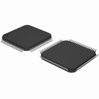
IC SERDES LVDS 16BIT BUS 80-LQFP
Manufacturer
National Semiconductor
Datasheet
1.DS92LV16TVHGNOPB.pdf
(19 pages)
Specifications of DS92LV16TVHG/NOPB
Function
Serializer/Deserializer
Data Rate
2.56Gbps
Input Type
LVTTL/LVCMOS
Output Type
LVTTL, LVCMOS
Number Of Inputs
1
Number Of Outputs
16
Voltage - Supply
3.15 V ~ 3.45 V
Operating Temperature
-40°C ~ 85°C
Mounting Type
Surface Mount
Package / Case
80-LQFP
No. Of Inputs
16
No. Of Outputs
16
Supply Voltage Range
3.15V To 3.45V
Driver Case Style
QFP
No. Of Pins
80
Msl
MSL 3 - 168 Hours
Filter Terminals
SMD
Rohs Compliant
Yes
Data Rate Max
1280Mbps
For Use With
BLVDS16EVK - BOARD EVAL FOR DS92LV16
Lead Free Status / RoHS Status
Lead free / RoHS Compliant
Other names
*DS92LV16TVHG
*DS92LV16TVHG/NOPB
DS92LV16TVHG
*DS92LV16TVHG/NOPB
DS92LV16TVHG
Available stocks
Company
Part Number
Manufacturer
Quantity
Price
Company:

Part Number:
DS92LV16TVHG/NOPB
Manufacturer:
NSC
Quantity:
251
Company:
Part Number:
DS92LV16TVHG/NOPB
Manufacturer:
Texas Instruments
Quantity:
10 000


Symbol
t
t
RNMI-R
t
t
RNMI-L
DSR1
DSR2
Deserializer Switching Characteristics
Over recommended operating supply and temperature ranges unless otherwise specified.
Note 1: “Absolute Maximum Ratings” are those values beyond which the safety of the device cannot be guaranteed. They are not meant to imply that the devices
should be operated at these limits. The table of “Electrical Characteristics” specifies conditions of device operation.
Note 2: Typical values are given for V
Note 3: Current into device pins is defined as positive. Current out of device pins is defined as negative. Voltages are referenced to ground except VOD, VOD,
VTH and VTL which are differential voltages.
Note 4: Due to TRI-STATE of the Serializer, the Deserializer will lose PLL lock and have to resynchronize before data transfer.
Note 5: For the purpose of specifying deserializer PLL performance tDSR1 and tDSR2 are specified with the REFCLK running and stable, and specific conditions
of the incoming data stream (SYNCPATs). It is recommended that the derserializer be initialized using either tDSR1 timing or tDSR2 timing. tDSR1 is the time
required for the deserializer to indicate lock upon power-up or when leaving the power-down mode. Synchronization patterns should be sent to the device before
initiating either condition. tDSR2 is the time required to indicate lock for the powered-up and enabled deserializer when the input (RI+ and RI-) conditions change
from not receiving data to receiving synchronization patterns (SYNCPATs).
Note 6: tRNMI is a measure of how much phase noise (jitter) the deserializer can tolerate in the incoming data stream before bit errors occur. It is a measurement
in reference with the ideal bit position, please see National’s AN-1217 for detail.
Note 7: Sync pattern is a fixed pattern with 8-bit of data high followed by 8-bit of data low.
Noise Margin Right
Noise Margin Left
Ideal Deserializer
Ideal Deserializer
Deserializer PLL
Deserializer PLL
PWRDWN (with
Lock Time from
Lock time from
SYNCPAT)
Parameter
SYNCPAT
CC
= 3.3V and T
Conditions
Figure 16
Figure 16
(Note 7)
(Note 6)
(Note 6)
A
= +25˚C.
Pin/Freq.
80 MHz
80 MHz
35 MHz
80 MHz
35 MHz
80 MHz
35MHz
35MHz
5
(Continued)
−630
−230
Min
Typ
3.7
1.9
1.5
0.9
+630
+230
Max
10
4
5
2
www.national.com
Units
µs
µs
µs
µs
ps
ps
ps
ps
Related parts for DS92LV16TVHG/NOPB
Image
Part Number
Description
Manufacturer
Datasheet
Request
R

Part Number:
Description:
National Semiconductor [8-Bit D/A Converter]
Manufacturer:
National Semiconductor
Datasheet:
Part Number:
Description:
National Semiconductor [Media Coprocessor]
Manufacturer:
National Semiconductor
Datasheet:
Part Number:
Description:
Digitally Controlled Tone and Volume Circuit with Stereo Audio Power Amplifier, Microphone Preamp Stage and National 3D Sound
Manufacturer:
National Semiconductor
Datasheet:
Part Number:
Description:
Digitally Controlled Tone and Volume Circuit with Stereo Audio Power Amplifier, Microphone Preamp Stage and National 3D Sound
Manufacturer:
National Semiconductor
Datasheet:
Part Number:
Description:
AC97 Rev 2 Codec with Sample Rate Conversion and National 3D Sound
Manufacturer:
National Semiconductor
Part Number:
Description:
Manufacturer:
National Semiconductor
Datasheet:
Part Number:
Description:
Manufacturer:
National Semiconductor
Datasheet:
Part Number:
Description:
General Purpose, Low Voltage, Low Power, Rail-to-Rail Output Operational Amplifiers
Manufacturer:
National Semiconductor
Datasheet:
Part Number:
Description:
8-bit 20 MSPS flash A/D converter.
Manufacturer:
National Semiconductor
Datasheet:
Part Number:
Description:
Low Noise Quad Operational Amplifier
Manufacturer:
National Semiconductor
Datasheet:
Part Number:
Description:
Quad Differential Line Receivers
Manufacturer:
National Semiconductor
Datasheet:
Part Number:
Description:
Quad High Speed Trapezoidal? Bus Transceiver
Manufacturer:
National Semiconductor
Datasheet:
Part Number:
Description:
Dual Line Receiver
Manufacturer:
National Semiconductor
Datasheet:
Part Number:
Description:
TTL to 10k ECL Level Translator with Latch
Manufacturer:
National Semiconductor
Datasheet: