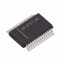
MAX9206EAI+ Maxim Integrated Products, MAX9206EAI+ Datasheet - Page 2

MAX9206EAI+
Manufacturer Part Number
MAX9206EAI+
Description
IC DESERIALIZER LVDS 28-SSOP
Manufacturer
Maxim Integrated Products
Datasheet
1.MAX9206EAI.pdf
(12 pages)
Specifications of MAX9206EAI+
Function
Deserializer
Data Rate
660Mbps
Input Type
LVDS
Output Type
LVTTL, LVCMOS
Number Of Inputs
1
Number Of Outputs
10
Voltage - Supply
3 V ~ 3.6 V
Operating Temperature
-40°C ~ 85°C
Mounting Type
Surface Mount
Package / Case
28-SSOP
Input Current
+/- 15 uA
Input Voltage Range (max)
3.6 V
Interface Type
Parallel LVCMOS/LVTTL
Maximum Operating Temperature
+ 85 C
Minimum Operating Temperature
- 40 C
Mounting Style
SMD/SMT
Operating Supply Voltage
3.3 V
Settling Time
3000 ps
Supply Voltage (max)
3.6 V
Supply Voltage (min)
3 V
Lead Free Status / RoHS Status
Lead free / RoHS Compliant
ABSOLUTE MAXIMUM RATINGS
AVCC, DVCC to AGND, DGND................................-0.3V to +4V
RI+, RI- to AGND, DGND .........................................-0.3V to +4V
All Other Pins to DGND ..............................-0.3V to DV
ROUT_ Short-Circuit Duration (Note 1) ......................Continuous
Continuous Power Dissipation (T
10-Bit Bus LVDS Deserializers
Stresses beyond those listed under “Absolute Maximum Ratings” may cause permanent damage to the device. These are stress ratings only, and functional
operation of the device at these or any other conditions beyond those indicated in the operational sections of the specifications is not implied. Exposure to
absolute maximum rating conditions for extended periods may affect device reliability.
DC ELECTRICAL CHARACTERISTICS
(V
-
T
2
A
POWER SUPPLY
Supply Current
Power-Down Supply Current
LVCMOS/LVTTL LOGIC INPUTS (REN, REFCLK, RCLK_R/F, PWRDN)
High-Level Input Voltage
Low-Level Input Voltage
Input Current
LVCMOS/LVTTL LOGIC OUTPUTS (ROUT_, RCLK, LOCK)
High-Level Output Voltage
Low-Level Output Voltage
Output Short-Circuit Current
Output High-Impedance Current
BLVDS SERIAL INPUT (RI+, RI-)
Differential Input High
Differential Input Low Threshold
Input Current
Power-Off Input Current
Input Resistor 1
Input Resistor 2
|
AVCC
V
28-Pin SSOP (derate 9.5mW/°C above +70°C) ..........762mW
= +25°C.) (Notes 2, 3)
ID
_______________________________________________________________________________________
/2
|
, T
= V
PARAMETER
A
DVCC
= -40°C to +85°C, unless otherwise noted. Typical values are at V
= +3.0V to +3.6V, differential input voltage
A
= +70°C)
SYMBOL
I
I
RI+
RI+OFF
I
RI-OFF
I
R
R
V
V
I
I
V
I
CCX
V
V
V
I
CC
OS
OZ
IN
OH
IN1
IN2
OL
TH
TL
, I
IH
IL
RI-
,
C
worst-case
pattern,
Figure 1
PWRDWN = low
V
I
I
V
PWRDN = low, V
= 0V, V
0.1V
0.45V < |V
0.1V
0.45V < |V
V
V
OH
OL
IN
ROUT_
AVCC
AVCC
L
= 15pF,
= 0V, V
= 5mA
= -5mA
CC
|V
= V
= V
|V
AVCC
= 0V
ID
+ 0.3V
ID
ID
ID
DVCC
DVCC
|
|
AVCC
|
|
, or V
0.45V
0.45V, V
CONDITIONS
0.6V
0.6V, V
MAX9206
MAX9208
, or V
= 3.6V or 0V, Figure 2
= 3.6V or 0V, Figure 2
|
ROUT_
V
DVCC
ID
|
DVCC
Operating Temperature Range ...........................-40°C to +85°C
Junction Temperature ......................................................+150°C
Storage Temperature Range .............................-65°C to +150°C
ESD Rating (Human Body Model, RI+, RI-) .........................±8kV
Lead Temperature (soldering, 10s) .................................+300°C
Soldering Temperature (reflow) .......................................+260°C
= 0.1V to 1.2V, common-mode voltage V
AVCC
AVCC
= V
RCLK
= V
= V
DVCC
DVCC
16MHz
45MHz
40MHz
60MHz
= V
AVCC
LOCK
= 0V
= 0V
= V
DVCC
-100
MIN
150
2.0
-15
2.2
-15
-64
-82
-64
-82
-1
0
0
4
= +3.3V, V
TYP
0.33
2.9
-38
30
57
55
80
-9
9
CM
CM
= 1.1V,
MAX
100
V
V
100
0.8
0.5
-85
45
75
75
15
64
82
64
82
=
CC
CC
1
1
|
V
|
ID
V
ID
/2
|
|
UNITS
= 0.2V,
to 2.4V
mA
mA
mA
mV
mV
k
k
μA
μA
μA
μA
V
V
V
V


