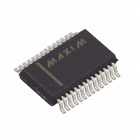
MAX9206EAI+ Maxim Integrated Products, MAX9206EAI+ Datasheet - Page 5

MAX9206EAI+
Manufacturer Part Number
MAX9206EAI+
Description
IC DESERIALIZER LVDS 28-SSOP
Manufacturer
Maxim Integrated Products
Datasheet
1.MAX9206EAI.pdf
(12 pages)
Specifications of MAX9206EAI+
Function
Deserializer
Data Rate
660Mbps
Input Type
LVDS
Output Type
LVTTL, LVCMOS
Number Of Inputs
1
Number Of Outputs
10
Voltage - Supply
3 V ~ 3.6 V
Operating Temperature
-40°C ~ 85°C
Mounting Type
Surface Mount
Package / Case
28-SSOP
Input Current
+/- 15 uA
Input Voltage Range (max)
3.6 V
Interface Type
Parallel LVCMOS/LVTTL
Maximum Operating Temperature
+ 85 C
Minimum Operating Temperature
- 40 C
Mounting Style
SMD/SMT
Operating Supply Voltage
3.3 V
Settling Time
3000 ps
Supply Voltage (max)
3.6 V
Supply Voltage (min)
3 V
Lead Free Status / RoHS Status
Lead free / RoHS Compliant
Figure 1. Worst-Case I
1, 12, 13
14, 20,
15–19,
21, 23
24–28
4, 11
PIN
10
22
2
3
5
6
7
8
9
ROUT
ROUT
RCLK
EVEN
ODD
RI
RCLK_R/F
REFCLK
ROUT9–
PWRDN
ROUT0
NAME
AGND
DGND
DVCC
AVCC
LOCK
RCLK
START
REN
RI+
BIT
RI-
_______________________________________________________________________________________
CC
0
Test Pattern
1
Analog Ground
Recovered Clock Strobe Edge Select. LVTTL/LVCMOS level input. Drive RCLK_ R/F high to strobe
ROUT_ on the rising edge of RCLK. Drive RCLK_R/F low to strobe ROUT_ on the falling edge of
RCLK.
PLL Reference Clock. LVTTL/LVCMOS level input.
Analog Power Supply. Bypass AVCC with a 0.1μF and a 0.001μF capacitor to AGND.
Serial Data Input. Noninverting BLVDS differential input.
Serial Data Input. Inverting BLVDS differential input.
Power Down. LVTTL/LVCMOS level input. Drive PWRDN low to stop the PLL and put ROUT_, LOCK,
and RCLK in high impedance.
Output Enable. LVTTL/LVCMOS level input. Drive REN low to put ROUT_ and RCLK in high
impedance. LOCK remains active, indicating the status of the serial input.
Recovered Clock. LVTTL/LVCMOS level output. Use RCLK to strobe ROUT_.
Lock Indicator. LVTTL/LVCMOS level output. LOCK goes low when the PLL has achieved frequency
and phase lock to the serial input, and the framing bits have been identified.
Digital Ground
Parallel Output Data. LVTTL/LVCMOS level outputs. ROUT_ is valid on the second selected strobe
edge of RCLK after LOCK goes low.
Digital Power Supply. Bypass DVCC with a 0.1μF and a 0.001μF capacitor to DGND.
2
3
4
5
RCLK_R/F = HIGH
6
7
10-Bit Bus LVDS Deserializers
8
9
T
DD
END
BIT
START
BIT
0
1
2
FUNCTION
Test Circuits/Timing Diagrams
3
4
5
6
7
8
9
END
BIT
Pin Description
START
BIT
0
1
2
5


