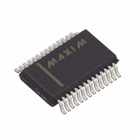
MAX9206EAI+ Maxim Integrated Products, MAX9206EAI+ Datasheet - Page 4

MAX9206EAI+
Manufacturer Part Number
MAX9206EAI+
Description
IC DESERIALIZER LVDS 28-SSOP
Manufacturer
Maxim Integrated Products
Datasheet
1.MAX9206EAI.pdf
(12 pages)
Specifications of MAX9206EAI+
Function
Deserializer
Data Rate
660Mbps
Input Type
LVDS
Output Type
LVTTL, LVCMOS
Number Of Inputs
1
Number Of Outputs
10
Voltage - Supply
3 V ~ 3.6 V
Operating Temperature
-40°C ~ 85°C
Mounting Type
Surface Mount
Package / Case
28-SSOP
Input Current
+/- 15 uA
Input Voltage Range (max)
3.6 V
Interface Type
Parallel LVCMOS/LVTTL
Maximum Operating Temperature
+ 85 C
Minimum Operating Temperature
- 40 C
Mounting Style
SMD/SMT
Operating Supply Voltage
3.3 V
Settling Time
3000 ps
Supply Voltage (max)
3.6 V
Supply Voltage (min)
3 V
Lead Free Status / RoHS Status
Lead free / RoHS Compliant
10-Bit Bus LVDS Deserializers
AC ELECTRICAL CHARACTERISTICS (continued)
(V
to 2.4V -
0.2V, T
Note 1: Short one output at a time. Do not exceed the Absolute Maximum continuous power dissipation.
Note 2: Current into a pin is defined as positive. Current out of a pin is defined as negative. Voltages are referenced to ground
Note 3: DC parameters are production tested at T
Note 4: AC parameters guaranteed by design and characterization.
Note 5: C
Note 6: t
4
AVCC
Input Jitter Tolerance
PLL Lock Time (from Start of
Sync Patterns)
LOCK High-Z to High-State
Delay
_______________________________________________________________________________________
A
= V
except V
ature range.
cy of TCLK must be within ±400ppm of the REFCLK frequency.
= +25°C.) (Notes 4, 5)
RCP
|
V
L
ID
DVCC
PARAMETER
includes scope probe and test jig capacitance.
/2
is determined by the period of TCLK, which is the reference clock of the serializer driving the deserializer. The frequen-
|
, T
TH
= +3.0V to +3.6V, C
A
, V
= -40°C to +85°C, unless otherwise noted. Typical values are at V
TL
, and V
ID
, which are differential input voltages.
SYMBOL
L
t
t
DSR2
ZHLK
= 15pF, differential input voltage
t
JT
Figure 7
PLL locked to stable REFCLK; supply
stable; static input; measured from
start of sync patterns at input to LOCK
transition low; Figure 8
Figure 9
A
= +25°C and guaranteed by design and characterization over operating temper-
CONDITIONS
MAX9206
MAX9208
|
V
ID
|
= 0.15V to 1.2V, common-mode voltage V
16MHz
45MHz
40MHz
60MHz
AVCC
1300
= V
MIN
720
720
320
DVCC
= +3.3V, V
TYP
42 x t
CM
MAX
30
RFCP
= 1.1V,
CM
=
UNITS
|
|
V
ns
ns
ps
V
ID
ID
|
/2
=
|


