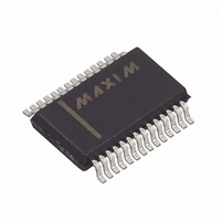
MAX9206EAI+ Maxim Integrated Products, MAX9206EAI+ Datasheet - Page 9

MAX9206EAI+
Manufacturer Part Number
MAX9206EAI+
Description
IC DESERIALIZER LVDS 28-SSOP
Manufacturer
Maxim Integrated Products
Datasheet
1.MAX9206EAI.pdf
(12 pages)
Specifications of MAX9206EAI+
Function
Deserializer
Data Rate
660Mbps
Input Type
LVDS
Output Type
LVTTL, LVCMOS
Number Of Inputs
1
Number Of Outputs
10
Voltage - Supply
3 V ~ 3.6 V
Operating Temperature
-40°C ~ 85°C
Mounting Type
Surface Mount
Package / Case
28-SSOP
Input Current
+/- 15 uA
Input Voltage Range (max)
3.6 V
Interface Type
Parallel LVCMOS/LVTTL
Maximum Operating Temperature
+ 85 C
Minimum Operating Temperature
- 40 C
Mounting Style
SMD/SMT
Operating Supply Voltage
3.3 V
Settling Time
3000 ps
Supply Voltage (max)
3.6 V
Supply Voltage (min)
3 V
Lead Free Status / RoHS Status
Lead free / RoHS Compliant
into high impedance but LOCK continues to reflect the
status of the serial input. Driving REN high again
enables the ROUT_ and RCLK drivers.
If one embedded clock edge (rising edge formed by
end/start bits) is not detected, LOCK goes high, RCLK
tracks REFCLK, and ROUT_ stays active but with
invalid data. LOCK stays high for a minimum of two
RCLK cycles. Then, if transitions are detected at the
serial input, the PLL attempts to lock to the serial input.
When the PLL locks to serial input data, LOCK goes
low, RCLK tracks the serializer reference clock (TCLK),
and ROUT_ is valid on the second selected strobe
edge of RCLK after LOCK goes low. A minimum of two
embedded clock edges in a row are required to regain
lock to the serial input after LOCK goes high.
For automatic resynchronization, LOCK can be con-
nected to the MAX9205/MAX9207 serializer SYNC1 or
SYNC2 input. With this connection, when LOCK goes
high, the serializer sends sync patterns until the deseri-
alizer locks to the serial input and drives LOCK low.
When the serial input is undriven (a disconnected cable
or serializer output in high impedance, for example) an
on-chip fail-safe circuit (Figure 2) drives the serial input
high. The response time of the fail-safe circuit depends
on interconnect characteristics. With an undriven input,
LOCK may switch high and low until the fail-safe circuit
takes effect. The undriven condition of the link can be
Table 1. Typical Lock Times
Note: Pseudorandom lock performed with 2 15 -1 PRBS pattern, 10,000 lock time tests.
Maximum
Maximum (Clock
Cycles)
Average
Average (Clock
Cycles)
Minimum
Minimum (Clock
Cycles)
FREQUENCY
PATTERN
REFCLK
DATA
_______________________________________________________________________________________
Losing Lock on Serial Data
PSEUDORANDOM
0.749μs
0.318μs
16MHz
0.13μs
DATA
11.99
5.09
2.08
Input Fail-Safe
10-Bit Bus LVDS Deserializers
PSEUDORANDOM
0.375μs
0.158μs
0.068μs
35MHz
DATA
13.14
5.52
2.37
detected in spite of LOCK switching since LOCK is
high long enough to be sampled (LOCK is high for at
least two RCLK cycles after a missed clock edge and
RCLK keeps running, allowing sampling). If it is
required that LOCK remain high for an undriven input,
the on-chip fail-safe circuit can be supplemented with
external pullup bias resistors.
The t
jitter the deserializer can tolerate before a sampling
error occurs (Figure 9). Zero-to-peak jitter is measured
from the mean value of the deterministic jitter distribu-
tion. Sources of jitter include the serializer (supply
noise, reference clock jitter, pulse skew, and intersym-
bol interference), the interconnect (intersymbol interfer-
ence, crosstalk, within-pair skew, ground shift), and the
deserializer (supply noise). The sum of the zero-to-peak
individual jitter sources must be less than or equal to
the minimum value of t
For example, at 40MHz, the MAX9205 serializer has
140ps (p-p) maximum deterministic output jitter. The
zero-to-peak value is 140ps/2 = 70ps. If the intercon-
nect jitter is 100ps (p-p) with a symmetrical distribution,
the zero-to-peak jitter is 50ps. The MAX9206 deserializ-
er jitter tolerance is 720ps at 40MHz. The total zero-to-
peak input jitter is 70ps + 50ps = 120ps, which is less
than the jitter tolerance. In this case, the margin is
720ps - 120ps = 600ps.
JT
parameter specifies the total zero-to-peak input
PSEUDORANDOM
0.354μs
0.144μs
0.061μs
40MHz
DATA
14.18
5.76
2.44
Deserializer Jitter Tolerance
JT
.
PATTERNS
0.134μs
0.103μs
0.061μs
40MHz
SYNC
5.37
4.11
2.45
9


