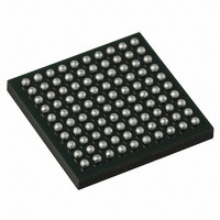
PI2EQX5804CNJE Pericom Semiconductor, PI2EQX5804CNJE Datasheet - Page 12

PI2EQX5804CNJE
Manufacturer Part Number
PI2EQX5804CNJE
Description
IC PCI-E REDRIVER 100LBGA
Manufacturer
Pericom Semiconductor
Series
ReDriver™r
Type
Redriverr
Datasheet
1.PI2EQX5804CNJE.pdf
(23 pages)
Specifications of PI2EQX5804CNJE
Tx/rx Type
CML
Capacitance - Input
50pF
Voltage - Supply
1.15 V ~ 1.25 V
Current - Supply
800mA
Mounting Type
Surface Mount
Package / Case
100-LBGA
Operating Temperature (min)
0C
Operating Temperature Classification
Commercial
Operating Temperature (max)
70C
Rad Hardened
No
Lead Free Status / RoHS Status
Lead free / RoHS Compliant
Delay Time
-
Lead Free Status / Rohs Status
Details
Available stocks
Company
Part Number
Manufacturer
Quantity
Price
Company:
Part Number:
PI2EQX5804CNJE
Manufacturer:
Pericom
Quantity:
1 453
Part Number:
PI2EQX5804CNJE
Manufacturer:
PERICOM
Quantity:
20 000
Part Number:
PI2EQX5804CNJEX
Manufacturer:
PERICOM
Quantity:
20 000
Register Description
Byte 0 - Signal Detect (SIG)
SIG_xy=0=low input signal, SIG_xy=1=valid input signal
Note: R=Read only, W=Write only, R/W=Read and Write, X=Undefi ned, rsvd=reserved for future use
The Signal Detect register provides information on the instantaneous status of the channel input from the Input Level
Threshold Detect circuit. If the input level falls below the Vth- level the relevant SIG_xy bit will be 0, indicating a low-
level noise or electrical idle input, resulting in the outputs going to the high-impedance off state or squelch mode. If the
input level is above Vth-, then SIG_xy is 1, indicating a valid input signal, and active signal recovery operation.
Byte 1 - Receiver Detect Output Register (RX50)
LB_xyxy#=0=loopback mode, LB_xyxy#=1=normal mode, DE_x=0=pre-emphasis, DE_x=1=de-emphasis
Note: R=Read only, W=Write only, R/W=Read and Write, X=Undefi ned, rsvd=reserved for future use
The RX50_xy bits report the result of a receiver detection cycle. One bit is assigned for each channel of the device.
RX50_xy is at a logic 1 level indicating a load and receiver was detected. When RX50_xy is 0 then a load device was
not detected. The RX50 register is read-only, and is undefi ned after power-up until a Receiver Detection cycle com-
pletes.
Byte 2 - Loopback and Emphasis Control Register (LBEC)
LB_xyxy#=0=loopback mode, LB_xyxy#=1=normal mode, DE_x=0=pre-emphasis, DE_x=1=de-emphasis
Note: R=Read only, W=Write only, R/W=Read and Write, X=Undefi ned, rsvd=reserved for future use
Individual control for each lane is provided for the loopback function via this register.
Power-on
Power-on
Power-on
Name
Name
Name
Type
State
Type
State
Type
State
Bit
Bit
Bit
09-0001
LB_A0B0#
RX50_A0
SIG_A0
R/W
LB#
R
X
R
X
7
7
7
LB_A1B1#
RX50_B0
SIG_B0
R/W
LB#
X
X
R
R
6
6
6
LB_A2B2#
RX50_A1
SIG_A1
R/W
LB#
X
X
R
R
5
5
5
LB_A3B3#
RX50_B1
SIG_B1
R/W
LB#
12
X
X
R
R
4
4
4
RX50_A2
5.0Gbps 4-Lane PCIe® 2.0 ReDriver™ with
SIG_A2
DE_A
DE_A
R/W
X
X
R
R
3
3
3
RX50_B2
SIG_B2
DE_B
DE_B
R/W
X
X
R
R
2
2
2
Equalization & Emphasis
RX50_A3
SIG_A3
rsvd
X
R
X
R
X
R
1
1
1
PS8926B
PI2EQX5804C
RX50_B3
SIG_B3
rsvd
X
R
X
R
X
R
0
0
0
06/08/09


