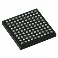
PI2EQX5804CNJE Pericom Semiconductor, PI2EQX5804CNJE Datasheet - Page 9

PI2EQX5804CNJE
Manufacturer Part Number
PI2EQX5804CNJE
Description
IC PCI-E REDRIVER 100LBGA
Manufacturer
Pericom Semiconductor
Series
ReDriver™r
Type
Redriverr
Datasheet
1.PI2EQX5804CNJE.pdf
(23 pages)
Specifications of PI2EQX5804CNJE
Tx/rx Type
CML
Capacitance - Input
50pF
Voltage - Supply
1.15 V ~ 1.25 V
Current - Supply
800mA
Mounting Type
Surface Mount
Package / Case
100-LBGA
Operating Temperature (min)
0C
Operating Temperature Classification
Commercial
Operating Temperature (max)
70C
Rad Hardened
No
Lead Free Status / RoHS Status
Lead free / RoHS Compliant
Delay Time
-
Lead Free Status / Rohs Status
Details
Available stocks
Company
Part Number
Manufacturer
Quantity
Price
Company:
Part Number:
PI2EQX5804CNJE
Manufacturer:
Pericom
Quantity:
1 453
Part Number:
PI2EQX5804CNJE
Manufacturer:
PERICOM
Quantity:
20 000
Part Number:
PI2EQX5804CNJEX
Manufacturer:
PERICOM
Quantity:
20 000
Confi guration Register Summary
3.3V to 1.2V Bi-directional Level Shifter
If the I
bus system, each section with a different supply voltage and different logic levels. In the bus system of Figure
2 the left section has pull-up resistors and devices connected to a 1.2 Volt supply voltage, the right section has
pull-up resistors and devices connected to a 3.3 Volt supply voltage. The devices of each section have I/O’s
with supply voltage related logic input levels and an open drain output confi guration.
The level shifter for each bus line is identical and consists of one discrete N-channel enhancement MOS-FET,
T1 for the serial data line SDA and T2 for the serial clock line SCL. The gates (g) has to be connected to the
lowest supply voltage VDD1 (1.2V), the sources (s) to the bus lines of the “Lower voltage” section, and the
drains (d) to the bus lines of the “Higher voltage” section. The diode between the drain (d) and substrate is
inside the MOS-FET present as n-p junction of drain and substrate.
7-bit addressing mode. The data byte format is 8 bit bytes. The bytes must be accessed in sequential order
from the lowest to the highest byte with the ability to stop after any complete byte has been transferred. Ad-
dress bits A4, A1 and A0 are programmable to support multiple chips environment. The data is loaded until a
Stop sequence is issued.
I
The integrated I
Byte
0
1
2
3
4
5
6
7
8
9
10
11
2
C Operation
2
09-0001
Mnemonic
SIG
RX50
LBEC
INDIS
OUTDIS
RESET
PWR
RXDE
AEOC
AEOC
RSVD
RSVD
C controller is 3.3V bus, the bi-directional level shifter is used to interconnect two sections of an I
2
C interface operates as a slave device, supporting standard rate operation of 100Kbps, with
Function
Signal Detect, indicates valid input signal level
Receiver Detect Output, indicates whether a receiver load was detected
Loopback and Emphasis Control, provides for control of the loopback function and emphasis mode (pre-
emphasis or de-emphasis)
Channel Input Disable, controls whether s channels input buffer is enabled or disabled
Channel Output Disable: Controls whether a channels output buffer is enabled or disabled
Channel Reset
Power Down Control, enables power down for each channel individually
Receiver Detect Enable, controls the receiver detect operation
A-Channels Equalizer and Output Control
B-Channels Equalizer and Output Control
Reserved
Reserved
9
5.0Gbps 4-Lane PCIe® 2.0 ReDriver™ with
Equalization & Emphasis
PS8926B
PI2EQX5804C
2
06/08/09
C-


