SCLT3-8BT8 STMicroelectronics, SCLT3-8BT8 Datasheet - Page 10
SCLT3-8BT8
Manufacturer Part Number
SCLT3-8BT8
Description
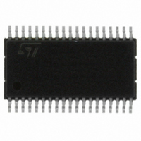
IC SERIAL TERM 8-LINE 38HTSSOP
Manufacturer
STMicroelectronics
Type
Serialr
Datasheet
1.SCLT3-8BT8.pdf
(33 pages)
Specifications of SCLT3-8BT8
Number Of Terminations
8
Voltage - Supply
9 V ~ 35 V
Operating Temperature
-25°C ~ 85°C
Mounting Type
Surface Mount
Package / Case
38-TSSOP Exposed Pad, 38-eTSSOP, 38-HTSSOP
Number Of I/os
8
Operating Supply Voltage
9 V to 35 V
Supply Current (max)
2.3 mA
Maximum Operating Temperature
+ 85 C
Minimum Operating Temperature
- 25 C
Mounting Style
SMD/SMT
Data Bus Width
8 bit, 16 bit
Lead Free Status / RoHS Status
Lead free / RoHS Compliant
Other names
497-10100-5
Available stocks
Company
Part Number
Manufacturer
Quantity
Price
Company:

Part Number:
SCLT3-8BT8
Manufacturer:
AD
Quantity:
6 259


Functional description
2.5
2.5.1
2.5.2
2.5.3
2.5.4
10/33
SPI bus signal description
Chip select /CS
When the chip select signal /CS is high, the data transfer is disabled (SCK and MOSI
signals are ignored) and the data output MISO is in high impedance tri-state Z.
Driving this input low enables the communication process. At each falling edge of the /CS,
the 8 input logic states, and the 8 control bits are loaded into the SPI shift register.
The chip select /CS must toggle only when the serial clock signal SCK is in low state.
Serial clock SCK
This clock signal defines the speed and sequence of the SPI communication and is
controlled by the master unit. Its transient edges define the serial protocol operation:
●
●
The SCLT internal circuitry secures the SPI operation in mode C
the chip select /CS falls low, the first edge of the clock SCK to be active is always the rising
edge.
Figure 8.
Serial data input MOSI
This input signal MOSI is used to shift external data bits into the SCLT register from the
most significant (MSB) bit to the least significant one (LSB). The data bits are captured by
the SCLT on the rising edge of the serial clock signal SCK.
Like the clock SCK, and the chip select /CS, the MOSI input circuit is filtered as shown in
Figure
of the SPI circuit.
Serial data output MISO
This output signal is used to transfer data out of the SCLT slave circuit from the most
significant bit (MSB) to the least significant bit (LSB). The first data bit is written out when
the chip select /CS goes low. Then the other data bits are written out on the falling edge of
the clock signal SCK.
The output MISO goes to high impedance tri-state shown on
goes in high state.
The falling edge generates the shift of the data in the register and the last bit writing on
the output MISO.
The rising edge generates the capture of the data on the input MOSI.
8, in order to match maximum speed operation and improve the EFT burst immunity
Functional diagram of the SPI logic inputs SCK, MOSI, /CS
SCK
Doc ID 15191 Rev 3
ESD HBM
2kΩ
250kΩ
V
DD
2pF
SCLT3-8
Table 5
POL
= 0, C
when the /CS signal
PHA
SCLT3-8BT8
= 0. When
Related parts for SCLT3-8BT8
Image
Part Number
Description
Manufacturer
Datasheet
Request
R

Part Number:
Description:
Protected Digital Input Termination With Serialized State Transfer
Manufacturer:
STMicroelectronics
Datasheet:
Part Number:
Description:
STMicroelectronics [RIPPLE-CARRY BINARY COUNTER/DIVIDERS]
Manufacturer:
STMicroelectronics
Datasheet:
Part Number:
Description:
STMicroelectronics [LIQUID-CRYSTAL DISPLAY DRIVERS]
Manufacturer:
STMicroelectronics
Datasheet:

Part Number:
Description:
BOARD EVAL FOR MEMS SENSORS
Manufacturer:
STMicroelectronics
Datasheet:
Part Number:
Description:
NPN TRANSISTOR POWER MODULE
Manufacturer:
STMicroelectronics
Datasheet:
Part Number:
Description:
TURBOSWITCH ULTRA-FAST HIGH VOLTAGE DIODE
Manufacturer:
STMicroelectronics
Datasheet:
Part Number:
Description:
Manufacturer:
STMicroelectronics
Datasheet:
Part Number:
Description:
DIODE / SCR MODULE
Manufacturer:
STMicroelectronics
Datasheet:
Part Number:
Description:
DIODE / SCR MODULE
Manufacturer:
STMicroelectronics
Datasheet:
Part Number:
Description:
Search -----> STE16N100
Manufacturer:
STMicroelectronics
Datasheet:
Part Number:
Description:
Search ---> STE53NA50
Manufacturer:
STMicroelectronics
Datasheet:
Part Number:
Description:
NPN Transistor Power Module
Manufacturer:
STMicroelectronics
Datasheet: