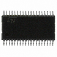
SCLT3-8BT8 STMicroelectronics, SCLT3-8BT8 Datasheet - Page 26

SCLT3-8BT8
Manufacturer Part Number
SCLT3-8BT8
Description
IC SERIAL TERM 8-LINE 38HTSSOP
Manufacturer
STMicroelectronics
Type
Serialr
Datasheet
1.SCLT3-8BT8.pdf
(33 pages)
Specifications of SCLT3-8BT8
Number Of Terminations
8
Voltage - Supply
9 V ~ 35 V
Operating Temperature
-25°C ~ 85°C
Mounting Type
Surface Mount
Package / Case
38-TSSOP Exposed Pad, 38-eTSSOP, 38-HTSSOP
Number Of I/os
8
Operating Supply Voltage
9 V to 35 V
Supply Current (max)
2.3 mA
Maximum Operating Temperature
+ 85 C
Minimum Operating Temperature
- 25 C
Mounting Style
SMD/SMT
Data Bus Width
8 bit, 16 bit
Lead Free Status / RoHS Status
Lead free / RoHS Compliant
Other names
497-10100-5
Available stocks
Company
Part Number
Manufacturer
Quantity
Price
Company:
Part Number:
SCLT3-8BT8
Manufacturer:
AD
Quantity:
6 259
Application considerations
3.3
3.4
26/33
Reverse polarity robustness
Any reverse polarity of an input IN
not disturb the operation of the other input channels as long as the power supply is working
properly (V
Such a case is not dissipative for the SCLT, < 15 mW per input, but consideration should be
given to the input resistors. A resistance of R
0.38 W at V
duration of this situation.
The power supply V
Surge voltage immunity
Figure 20. Surge voltage test diagram of the SCLT circuit
The input and supply pins are designed to withstand electromagnetic interferences. They
are protected by a clamping function that is connected to the ground pin COM
with the serial input resistance R
transient bursts (± 4 kV, IEC 61000-4-4) and the voltage surges (± 1 kV, IEC 61000-4-5).
This topology allows the surge voltage to be applied from each input to other inputs, the
ground and the supply contacts in differential or common modes as shown on
Thanks to its high resistance R
according to IEC 61000-4-5 using same diagram as
supply pin withstands more than ± 2.5 kV.
CC
I
V
V
V
V
= 30 V. The dissipation rating of the input resistor is set according to the
PPS
PPS
PPS
PPS
>19 V).
= +/- 1kV with 2 Ω
= +/- 1kV with 2
C
V
V
V
V
PPI
PPI
withstands also this kind of stress, the whole circuit being disabled.
PPI
PPI
I
I
GND
GND
PE/FE
PE/FE
V
V
PPI
PPI
Doc ID 15191 Rev 3
C
= +/- 1kV with 42 Ω
= +/- 1kV with 42
I
= 500 Ω, the supply pin V
, this clamping protection is effective against the fast
I
generates some negative current in the circuit that does
V
V
V
PP
PP
PP
5 nF
5 nF
IN
= 2.2 kΩ should produce a dissipation of
V
V
CC
CC
Figure
C
R
R
R
R
R
R
R
R
20. With R
C
C
I
I
I
I
I
I
withstands ±1 kV surge voltage
COM
COM
V
V
IN
IN
IN
IN
SCLT3-8
SCLT3-8
C
C
1
1
2
2
C
P
P
= 2.2 kΩ, this power
P
SCLT3-8BT8
Figure
. Combined
20.


