SCLT3-8BT8 STMicroelectronics, SCLT3-8BT8 Datasheet - Page 15
SCLT3-8BT8
Manufacturer Part Number
SCLT3-8BT8
Description
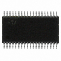
IC SERIAL TERM 8-LINE 38HTSSOP
Manufacturer
STMicroelectronics
Type
Serialr
Datasheet
1.SCLT3-8BT8.pdf
(33 pages)
Specifications of SCLT3-8BT8
Number Of Terminations
8
Voltage - Supply
9 V ~ 35 V
Operating Temperature
-25°C ~ 85°C
Mounting Type
Surface Mount
Package / Case
38-TSSOP Exposed Pad, 38-eTSSOP, 38-HTSSOP
Number Of I/os
8
Operating Supply Voltage
9 V to 35 V
Supply Current (max)
2.3 mA
Maximum Operating Temperature
+ 85 C
Minimum Operating Temperature
- 25 C
Mounting Style
SMD/SMT
Data Bus Width
8 bit, 16 bit
Lead Free Status / RoHS Status
Lead free / RoHS Compliant
Other names
497-10100-5
Available stocks
Company
Part Number
Manufacturer
Quantity
Price
Company:

Part Number:
SCLT3-8BT8
Manufacturer:
AD
Quantity:
6 259


SCLT3-8BT8
2.7.4
2.7.5
It is supposed such disturbances affect one bit at a time during the SPI frame transfer. EFT
burst repetition rate is about 200 µs (5 kHz) and the SPI 16-bit frame should last less than
160 µs.
A parity bit on the full byte should be obtained by applying an “exclusive NOR” Boolean
operation to the eight logic input states (PC
even.
The other parity bits PC2 and PC3 are obtained with an “exclusive NOR” Boolean operation
respectively on the MSB half data byte (IN
and PC
considered inputs is even.
These parity bits allow one error to be detected at a time in the SPI data transfer, and this
error can be corrected thanks to a second SPI data scan because the corrupted data bit
should be statistically different between the two scan sequences.
A method is proposed to correct one corrupted input data bit. If full data byte parity bit PC
wrong, the first scanned word is stored, and the SCLT input data are scanned immediately
twice. Then the first full byte parity bit is checked with its half byte parity bits to confirm the
error. The second scanned SPI word is stored and its full byte parity bit is also checked.
By using the parity bits on half data byte (the 4 MSB, the 4 LSB, the 4 medium bits), the
corrupted input data bit couple of the two scanned SPI words can be detected and the input
data byte can be re-synthesized by isolating and replacing these failing bit couples.
SPI hardware interface
All the logic level output signals deliver 80% of V
This SPI circuit is designed to drive CMOS circuit or isolated opto-transistors. Since the
clock frequency is always higher than 100 kHz, high speed opto-transistors are selected
requiring higher driving input and output currents.
The biasing resistors of their output transistors are kept external to allow the speed and the
device sourcing to be set for each application, providing thus more flexibility in the choice of
these isolators.
In
applications.
Loss of V
The operation of the SCLT is extended beyond the levels required in the IEC 61131-2
standard to allow the implementation of the under voltage alarm UVA as described in
Section
If there is no more power feeding on the V
the MISO output is forced in low state during SPI transfer attempt. The last SPI control data
bit is a stop bit placed normally in high state. The loss of power supply is detected by
checking its state. If low, the output is disabled by the internal power reset POR.
This POR signal is active in low state when V
V
DD
Section 3: Application
is less than 3.25 V.
4
2.7.1.
on the middle half data byte (IN
CC
power supply
considerations, several cases are proposed for the major
Doc ID 15191 Rev 3
3
CC
5
to IN
1
to IN
): it goes high when the parity of the 8 inputs is
C
input, the SCLT chip goes to sleep mode, and
6
is less than 9 V or the internal power supply
): they go high when the parity of the 4
DD
8
) and the LSB half data byte (IN1 to IN
for high state and 20% V
Functional description
DD
for low state.
15/33
1
4
),
is
Related parts for SCLT3-8BT8
Image
Part Number
Description
Manufacturer
Datasheet
Request
R

Part Number:
Description:
Protected Digital Input Termination With Serialized State Transfer
Manufacturer:
STMicroelectronics
Datasheet:
Part Number:
Description:
STMicroelectronics [RIPPLE-CARRY BINARY COUNTER/DIVIDERS]
Manufacturer:
STMicroelectronics
Datasheet:
Part Number:
Description:
STMicroelectronics [LIQUID-CRYSTAL DISPLAY DRIVERS]
Manufacturer:
STMicroelectronics
Datasheet:

Part Number:
Description:
BOARD EVAL FOR MEMS SENSORS
Manufacturer:
STMicroelectronics
Datasheet:
Part Number:
Description:
NPN TRANSISTOR POWER MODULE
Manufacturer:
STMicroelectronics
Datasheet:
Part Number:
Description:
TURBOSWITCH ULTRA-FAST HIGH VOLTAGE DIODE
Manufacturer:
STMicroelectronics
Datasheet:
Part Number:
Description:
Manufacturer:
STMicroelectronics
Datasheet:
Part Number:
Description:
DIODE / SCR MODULE
Manufacturer:
STMicroelectronics
Datasheet:
Part Number:
Description:
DIODE / SCR MODULE
Manufacturer:
STMicroelectronics
Datasheet:
Part Number:
Description:
Search -----> STE16N100
Manufacturer:
STMicroelectronics
Datasheet:
Part Number:
Description:
Search ---> STE53NA50
Manufacturer:
STMicroelectronics
Datasheet:
Part Number:
Description:
NPN Transistor Power Module
Manufacturer:
STMicroelectronics
Datasheet: