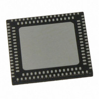
PI7C9X20303ULAZPE Pericom Semiconductor, PI7C9X20303ULAZPE Datasheet - Page 35

PI7C9X20303ULAZPE
Manufacturer Part Number
PI7C9X20303ULAZPE
Description
IC PCIE PACKET SWITCH 132VQFN
Manufacturer
Pericom Semiconductor
Series
UltraLo™r
Specifications of PI7C9X20303ULAZPE
Applications
Data Transport
Interface
Advanced Configuration Power Interface (ACPI)
Package / Case
132-VQFN
Mounting Type
Surface Mount
Lead Free Status / RoHS Status
Lead free / RoHS Compliant
Voltage - Supply
-
Available stocks
Company
Part Number
Manufacturer
Quantity
Price
Company:
Part Number:
PI7C9X20303ULAZPE
Manufacturer:
LATTICE
Quantity:
33
Company:
Part Number:
PI7C9X20303ULAZPEX
Manufacturer:
TI
Quantity:
3
7.2.13
7.2.14
7.2.15
7.2.16
August 2009 – Revision 1.1
Pericom Semiconductor
SECONDARY LATENCY TIMER REGISTER – OFFSET 18h
I/O BASE ADDRESS REGISTER – OFFSET 1Ch
I/O LIMIT ADDRESS REGISTER – OFFSET 1Ch
SECONDARY STATUS REGISTER – OFFSET 1Ch
BIT
31:24
BIT
3:0
7:4
BIT
11:8
15:12
BIT
20:16
21
22
23
24
26:25
27
28
FUNCTION
Secondary Latency
Timer
FUNCTION
32-bit Indicator
I/O Base Address
[15:12]
FUNCTION
32-bit Indicator
I/O Limit Address
[15:12]
FUNCTION
Reserved
66MHz Capable
Reserved
Fast Back-to-Back
Capable
Master Data Parity
Error
DEVSEL_L timing
Signaled Target
Abort
Received Target
Abort
TYPE
TYPE
TYPE
TYPE
RWC
RW
RW
RO
RO
RO
RO
RO
RO
RO
RO
RO
RO
Page 35 of 77
DESCRIPTION
Does not apply to PCI Express. Must be hardwired to 00h.
DESCRIPTION
Read as 01h to indicate 32-bit I/O addressing.
Defines the bottom address of the I/O address range for the Bridge to
determine when to forward I/O transactions from one interface to the other.
The upper 4 bits correspond to address bits [15:12] and are writable. The
lower 12 bits corresponding to address bits [11:0] are assumed to be 0. The
upper 16 bits corresponding to address bits [31:16] are defined in the I/O base
address upper 16 bits address register.
Reset to 0h.
DESCRIPTION
Read as 01h to indicate 32-bit I/O addressing.
Defines the top address of the I/O address range for the Bridge to determine
when to forward I/O transactions from one interface to the other. The upper 4
bits correspond to address bits [15:12] and are writable. The lower 12 bits
corresponding to address bits [11:0] are assumed to be FFFh. The upper 16
bits corresponding to address bits [31:16] are defined in the I/O limit address
upper 16 bits address register.
Reset to 0h.
DESCRIPTION
Reset to 00000b.
Does not apply to PCI Express. Must be hardwired to 0b.
Reset to 0b.
Does not apply to PCI Express. Must be hardwired to 0b.
Set to 1 (by a requester) whenever a Parity error is detected or forwarded on
the secondary side of the port in a Switch.
If the Parity Error Response Enable bit is cleared, this bit is never set.
Reset to 0b.
Does not apply to PCI Express. Must be hardwired to 0b.
Set to 1 (by a completer) whenever completing a request in the secondary side
using Completer Abort Completion Status.
Reset to 0b.
Set to 1 (by a requestor) whenever receiving a Completion with Completer
Abort Completion Status in the secondary side.
Reset to 0b.
3Port-3Lane PCI Express® Switch
UltraLo
PI7C9X20303UL
Datasheet
TM
Family


