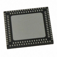
PI7C9X20303ULAZPE Pericom Semiconductor, PI7C9X20303ULAZPE Datasheet - Page 68

PI7C9X20303ULAZPE
Manufacturer Part Number
PI7C9X20303ULAZPE
Description
IC PCIE PACKET SWITCH 132VQFN
Manufacturer
Pericom Semiconductor
Series
UltraLo™r
Specifications of PI7C9X20303ULAZPE
Applications
Data Transport
Interface
Advanced Configuration Power Interface (ACPI)
Package / Case
132-VQFN
Mounting Type
Surface Mount
Lead Free Status / RoHS Status
Lead free / RoHS Compliant
Voltage - Supply
-
Available stocks
Company
Part Number
Manufacturer
Quantity
Price
Company:
Part Number:
PI7C9X20303ULAZPE
Manufacturer:
LATTICE
Quantity:
33
Company:
Part Number:
PI7C9X20303ULAZPEX
Manufacturer:
TI
Quantity:
3
9
An IEEE 1149.1 compatible Test Access Port (TAP) controller and associated TAP pins are provided to support
boundary scan in PI7C9X20303UL for board-level continuity test and diagnostics. The TAP pins assigned are TCK,
TDI, TDO, TMS and TRST_L. All digital input, output, input/output pins are tested except TAP pins.
9.1
The IEEE 1149.1 Test Logic consists of a TAP controller, an instruction register, and a group of test data registers
including Bypass and Boundary Scan registers. The TAP controller is a synchronous 16-state machine driven by the
Test Clock (TCK) and the Test Mode Select (TMS) pins. An independent power on reset circuit is provided to
ensure the machine is in TEST_LOGIC_RESET state at power-up.
PI7C9X20303UL implements a 5-bit Instruction register to control the operation of the JTAG logic. The defined
instruction codes are shown in Table 10-1. Those bit combinations that are not listed are equivalent to the BYPASS
(11111) instruction:
9.2
9.3
number for the device.
August 2009 – Revision 1.1
Pericom Semiconductor
The required bypass register (one-bit shift register) provides the shortest path between TDI and TDO when a
bypass instruction is in effect. This allows rapid movement of test data to and from other components on the
board. This path can be selected when no test operation is being performed on the PI7C9X20303UL.
IEEE 1149.1 COMPATIBLE JTAG CONTROLLER
INSTRUCTION REGISTER
BYPASS REGISTER
DEVICE ID REGISTER
Table 9-1 Instruction register codes
This register identifies Pericom as the manufacturer of the device and details the part number and revision
Table 9-2 JTAG device ID register
Instruction
EXTEST
SAMPLE
HIGHZ
CLAMP
IDCODE
BYPASS
INT_SCAN
MEM_BIST
Bit
31-28
27-12
11-1
0
Type
RO
RO
RO
RO
Operation Code (binary)
00000
00001
00101
00100
01100
11111
00010
01010
Value
0001
1001001000000100
01000111111
1
Register Selected
Boundary Scan
Boundary Scan
Bypass
Bypass
Device ID
Bypass
Internal Scan
Memory BIST
Page 68 of 77
Description
Version number
Last 4 digits (hex) of the die part number
Pericom identifier assigned by JEDEC
Fixed bit equal to 1’b1
Operation
Drives / receives off-chip test data
Samples inputs / pre-loads outputs
Tri-states output and I/O pins except TDO pin
Drives pins from boundary-scan register and selects Bypass
register for shifts
Accesses the Device ID register, to read manufacturer ID, part
number, and version number
Selected Bypass Register
Scan test
Memory BIST test
3Port-3Lane PCI Express® Switch
UltraLo
PI7C9X20303UL
Datasheet
TM
Family


