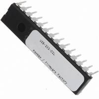
USB-232-DIL Flexipanel, USB-232-DIL Datasheet - Page 6

USB-232-DIL
Manufacturer Part Number
USB-232-DIL
Description
IC USB ASYNC SRL UART 28-DIL
Manufacturer
Flexipanel
Datasheet
1.USB-232-SS.pdf
(11 pages)
Specifications of USB-232-DIL
Applications
USB
Interface
I²C, SPI
Voltage - Supply
3.3 V ~ 5 V
Package / Case
28-DIP
Mounting Type
Through Hole
Lead Free Status / RoHS Status
Lead free / RoHS Compliant
Other names
658-1032-5
Both-powered Powered Device
If both self-powered and bus powered configurations are
possible, a circuit must be provided to switch over power
to USB power. An example sub-circuit is given in figure
4, where it is assumed that USB power is used when it
is available. To give self-power priority, place T2 so that
it switches the USB power line instead. D1 and D2
ensure that the two power lines are not in contention. If
the self-power source is 3.3V, the diodes will be
sufficient and T2 will not be required at all.
Power Take-Off
A device should only draw current from the USB line
once USB configuration is complete and the host PC is
not is sleep mode. The AllSysGo# output (active low)
can provide such a switch using the sub-circuit shown in
figure 5. C4 / R6 provide a slow switch-on to prevent
inrush current exceeding USB power limitations. 1μF
and 100nF smoothing capacitors are recommended on
both self and USB power lines. The Low Pwr output
should be monitored if the device can draw more than
100mA.
RS232 DTE Emulation
The familiar 9-pin D-shaped RS232 port on older PCs is
know as Data Terminal Emulator configuration.
means that TxD, RTS and DTR are outputs and RxD,
CTS, DSR, DCD and RI are inputs.
complete RS232 DTE implementation, a MAX239 is
used to convert to RS232 voltage levels, as shown in
figure 6. The MAX239 is suitable for Vdd = 5V circuits.
For Vdd = 3.3V, a MAX3241 should be used.
p6 of 11
USB-Power Vdd
Figure 4
Self-Power Vdd
3.3V - 5V
Vdd
Figure 3
USB-232
26-Aug-10
Vss
R1
C4
AllSysGo
USB Pwr Sns
R40
T1
R6
R30
USB Pwr
Sns
Vdd
Vss
T2
D+
D-
Self Power Source
USB-232
Vdd
D1
D2
R30
R40
Vss
Vdd
Vout
Figure 5
4
3
2
1
Self Pwr
Sns
USB
Vss
To provide a
R50
USB-232
This
RS232 without a signal inverter
It is possible to generate acceptable RS232 signal levels
parasitically without the use of a signal inverter chip.
The
limitations:
It is ideal for applications such as a low-cost command
line interface. See figure 6 for details.
Vdd
Vss
Vdd
(Active low shown)
GND
circuit for each input
RXD
DCD
One LED circuit
DTR
TXD
(Active low shown)
for each output
One pushbutton
Connector
PB1x
RS232
Hardware flow control is not implemented
Operation is half-duplex, i.e. you should not
When the remote device sends a byte, it is
The use of pull-up and pull-down resistors may
The remote device should have a ‘high’ signal
The resistor value shown would consumes higher
HW143-19
R2x
5
4
3
2
1
R1x
implementation
transmit while data is being received
automatically echoed back
limit the cable length below that normally
achievable
level greater than Vdd
current than is acceptable during standby.
9
8
6
7
RTS
DSR
RI
CTS
C8
Vdd
Vss
USB-232
C31
C32
Buff Empty
Tx Ind
Rx Ind
Reset#
DCD#
DSR#
RI#
Suspend
DTR#
AllSysGo#
Send
C7
Vusb
Vss
TEAclipper
connector
C1-
C2+
C2-
C1+
C6
TxD
RxD
C1
is
1
MAX239
Fig 7.
2
USB-232
3
Vss
subject
Vdd
4
4K7
5
Vdd
www.firmwarefactory.com
Vss
4K7
e.g. BSS138
e.g. BSS84
OSC2
OSC1
to
Gnd
Vcc
D+
D-
V+
V-
C33
C34
the
TxD232
RxD232
Vdd
Vss
X1
C3
Figure 6
C2
C35
following
Vdd
Vss
4
3
2
1
Vss
USB


