CD4051BCMX Fairchild Semiconductor, CD4051BCMX Datasheet
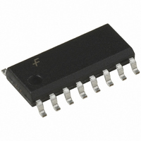
IC MUX/DEMUX 8X1 16SOIC

CD4051BCMX

Manufacturer Part Number
CD4051BCMX
Description
IC MUX/DEMUX 8X1 16SOIC
Manufacturer
Fairchild Semiconductor
Series
4000Br
Type
Analog Multiplexerr
Datasheet

Specifications of CD4051BCMX

Function
Multiplexer/Demultiplexer
Circuit
1 x 8:1
On-state Resistance
240 Ohm
Voltage Supply Source
Dual Supply
Voltage - Supply, Single/dual (±)
±5 V ~ 15 V
Current - Supply
20µA
Operating Temperature
-55°C ~ 125°C
Mounting Type
Surface Mount
Package / Case
16-SOIC (0.154", 3.90mm Width)
Multiplexer Configuration
Single 8:1
Number Of Inputs
8
Number Of Outputs
1
Number Of Channels
1
Analog Switch On Resistance
1050@5VOhm
Analog Switch Turn On Time
1.2us
Analog Switch Turn Off Time
420ns
Package Type
SOIC N
Power Supply Requirement
Single/Dual
Single Supply Voltage (min)
5V
Single Supply Voltage (typ)
9/12V
Single Supply Voltage (max)
15V
Dual Supply Voltage (min)
±2.5V
Dual Supply Voltage (typ)
±3/±5V
Dual Supply Voltage (max)
±7.5V
Power Dissipation
500mW
Mounting
Surface Mount
Pin Count
16
Operating Temp Range
-55C to 125C
Operating Temperature Classification
Military
On Resistance (max)
1050 Ohms
Propagation Delay Time
55 ns
On Time (max)
1200 ns
Off Time (max)
420 ns
Supply Voltage (max)
15 V
Supply Voltage (min)
5 V
Maximum Power Dissipation
500 mW
Maximum Operating Temperature
+ 125 C
Minimum Operating Temperature
- 55 C
Mounting Style
SMD/SMT
Number Of Switches
Single
No. Of Circuits
1
Supply Current
20µA
On State Resistance Max
1.05kohm
Supply Voltage Range
5V To 15V
Operating Temperature Range
-55°C To +125°C
Analog Switch Case Style
SOIC
Rohs Compliant
Yes
Lead Free Status / RoHS Status
Lead free / RoHS Compliant
Other names
CD4051BCMX
CD4051BCMXTR

Available stocks

Company
Part Number
Manufacturer
Quantity
Price
Part Number:
CD4051BCMX
Manufacturer:
NS/国半
Quantity:
20 000
© 2002 Fairchild Semiconductor Corporation
CD4051BCM
CD4051BCSJ
CD4051BCMTC
CD4051BCN
CD4052BCM
CD4052BCSJ
CD4052BCN
CD4053BCM
CD4053BCSJ
CD4053BCN
CD4051BC • CD4052BC • CD4053BC
Single 8-Channel Analog Multiplexer/Demultiplexer •
Dual 4-Channel Analog Multiplexer/Demultiplexer •
Triple 2-Channel Analog Multiplexer/Demultiplexer
General Description
The CD4051BC, CD4052BC, and CD4053BC analog mul-
tiplexers/demultiplexers are digitally controlled analog
switches having low “ON” impedance and very low “OFF”
leakage currents. Control of analog signals up to 15V
can be achieved by digital signal amplitudes of 3 15V. For
example, if V
nals from 5V to 5V can be controlled by digital inputs of
0 5V. The multiplexer circuits dissipate extremely low qui-
escent power over the full V
voltage ranges, independent of the logic state of the control
signals. When a logical “1” is present at the inhibit input ter-
minal all channels are “OFF”.
CD4051BC is a single 8-channel multiplexer having three
binary control inputs. A, B, and C, and an inhibit input. The
three binary signals select 1 of 8 channels to be turned
“ON” and connect the input to the output.
CD4052BC is a differential 4-channel multiplexer having
two binary control inputs, A and B, and an inhibit input. The
two binary input signals select 1 or 4 pairs of channels to
be turned on and connect the differential analog inputs to
the differential outputs.
CD4053BC is a triple 2-channel multiplexer having three
separate digital control inputs, A, B, and C, and an inhibit
input. Each control input selects one of a pair of channels
which are connected in a single-pole double-throw configu-
ration.
Ordering Code:
Devices also available in Tape and Reel. Specify by appending the suffix letter “X” to the ordering code.
Order Number
DD
5V, V
Package Number
SS
MTC16
M16D
M16D
M16D
M16A
N16E
M16A
N16E
M16A
N16E
0V and V
DD
V
SS
and V
EE
16-Lead Small Outline Package (SOP), EIAJ TYPE II, 5.3mm Wide
16-Lead Small Outline Integrated Circuit (SOIC), JEDEC MS-012, 0.150" Narrow
16-Lead Thin Shrink Small Outline Package (TSSOP), JEDEC MO-153, 4.4mm Wide
16-Lead Plastic Dual-In-Line Package (PDIP), JEDEC MS-001, 0.300" Wide
16-Lead Small Outline Integrated Circuit (SOIC), JEDEC MS-012, 0.150" Narrow
16-Lead Plastic Dual-In-Line Package (PDIP), JEDEC MS-001, 0.300" Wide
16-Lead Small Outline Integrated Circuit (SOIC), JEDEC MS-012, 0.150" Narrow
16-Lead Plastic Dual-In-Line Package (PDIP), JEDEC MS-001, 0.300" Wide
DD
5V, analog sig-
DS005662
V
EE
supply
p-p
Features
Wide range of digital and analog signal levels:
digital 3 – 15V, analog to 15V
Low “ON” resistance: 80 (typ.) over entire 15V
signal-input range for V
High “OFF” resistance:
channel leakage of 10 pA (typ.) at V
Logic level conversion for digital addressing signals of
3 – 15V (V
to 15 V
Matched switch characteristics:
Very low quiescent power dissipation under all
digital-control input and supply conditions:
1
Binary address decoding on chip
R
ON
W (typ.) at V
Package Description
p-p
5
(V
DD
(typ.) for V
DD
V
DD
SS
V
EE
V
DD
3 – 15V) to switch analog signals
SS
DD
15V)
V
V
V
November 1983
Revised April 2002
EE
p-p
DD
EE
15V
V
15V
EE
www.fairchildsemi.com
DD
10V
V
EE
p-p
10V

Related parts for CD4051BCMX

CD4051BCMX Summary of contents

Page 1

... N16E 16-Lead Plastic Dual-In-Line Package (PDIP), JEDEC MS-001, 0.300" Wide Devices also available in Tape and Reel. Specify by appending the suffix letter “X” to the ordering code. © 2002 Fairchild Semiconductor Corporation Features Wide range of digital and analog signal levels: digital 3 – 15V, analog to 15V Low “ ...

Page 2

Connection Diagrams Pin Assignments for DIP and SOIC CD4051BC Truth Table INPUT STATES INHIBIT *Don’t Care condition. www.fairchildsemi.com CD4052BC CD4053BC “ON” ...

Page 3

Logic Diagrams CD4051BC CD4052BC 3 www.fairchildsemi.com ...

Page 4

Logic Diagrams (Continued) www.fairchildsemi.com CD4053BC 4 ...

Page 5

Absolute Maximum Ratings DC Supply Voltage ( Input Voltage ( Storage Temperature Range ( Power Dissipation ( Dual-In-Line Small Outline Lead Temperature ( (soldering, 10 ...

Page 6

DC Electrical Characteristics Symbol Parameter Conditions Control Inputs and Inhibit V LOW Level Input Voltage all OFF Channels 10V ...

Page 7

AC Electrical Characteristics ns, unless otherwise specified Symbol Parameter t Propagation Delay Time from V PZH Inhibit to Signal Output R PZL L (channel turning on ...

Page 8

Special Considerations In certain applications the external load-resistor current may include both V and signal-line components avoid drawing V current when switch current flows into DD IN/OUT pin, the voltage drop across the bidirectional Typical Performance Characteristics “ON” ...

Page 9

Switching Time Waveforms 9 www.fairchildsemi.com ...

Page 10

Physical Dimensions inches (millimeters) unless otherwise noted 16-Lead Small Outline Integrated Circuit (SOIC), JEDEC MS-012, 0.150" Narrow www.fairchildsemi.com Package Number M16A 10 ...

Page 11

Physical Dimensions inches (millimeters) unless otherwise noted (Continued) 16-Lead Small Outline Package (SOP), EIAJ TYPE II, 5.3mm Wide Package Number M16D 11 www.fairchildsemi.com ...

Page 12

Physical Dimensions inches (millimeters) unless otherwise noted (Continued) 16-Lead Thin Shrink Small Outline Package (TSSOP), JEDEC MO-153, 4.4mm Wide www.fairchildsemi.com Package Number MTC16 12 ...

Page 13

Physical Dimensions inches (millimeters) unless otherwise noted (Continued) 16-Lead Plastic Dual-In-Line Package (PDIP), JEDEC MS-001, 0.300" Wide Fairchild does not assume any responsibility for use of any circuitry described, no circuit patent licenses are implied and Fairchild reserves the right ...

Related keywords