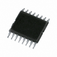
74LV4052PW,112 NXP Semiconductors, 74LV4052PW,112 Datasheet - Page 11

74LV4052PW,112
Manufacturer Part Number
74LV4052PW,112
Description
IC MUX/DEMUX DUAL 4X1 16TSSOP
Manufacturer
NXP Semiconductors
Series
74LVr
Type
Analog Multiplexerr
Datasheet
1.74LV4052DB118.pdf
(16 pages)
Specifications of 74LV4052PW,112
Function
Multiplexer/Demultiplexer
Circuit
2 x 4:1
On-state Resistance
60 Ohm
Voltage Supply Source
Single Supply
Voltage - Supply, Single/dual (±)
2.7 V ~ 3.6 V
Current - Supply
80µA
Operating Temperature
-40°C ~ 125°C
Mounting Type
Surface Mount
Package / Case
16-TSSOP (0.173", 4.40mm Width)
Multiplexer Configuration
Dual 4:1
Number Of Inputs
8
Number Of Outputs
2
Number Of Channels
2
Analog Switch On Resistance
250@1.2VOhm
Package Type
TSSOP
Power Supply Requirement
Single
Single Supply Voltage (min)
1V
Single Supply Voltage (typ)
3.3V
Single Supply Voltage (max)
6V
Dual Supply Voltage (min)
Not RequiredV
Dual Supply Voltage (typ)
Not RequiredV
Dual Supply Voltage (max)
Not RequiredV
Power Dissipation
400mW
Mounting
Surface Mount
Pin Count
16
Operating Temp Range
-40C to 125C
Operating Temperature Classification
Automotive
Lead Free Status / RoHS Status
Lead free / RoHS Compliant
Other names
74LV4052PW
74LV4052PW
935174950112
74LV4052PW
935174950112
1. V
2. V
3. V
Philips Semiconductors
WAVEFORMS
NOTES:
TEST CIRCUIT
1998 Jun 23
Dual 4-channel analog multiplexer/demultiplexer
V
the output load
V
V
V
Figure 13. Input (V
GENERATOR
M
M
OL
x
X
Y
Y
2.7 - 3.6V
= V
> 3.6 V
< 2.7V
= V
= V
= V
PULSE
= 1.5 V at 2.7 V
= 0.5
and V
OUTPUTS
V
OL
CC
OL
OH
OH
INPUTS
+ 0.3 V at 2.7 V
+ 0.1
V I
GND
V OH
– 0.3 V at 2.7 V
– 0.1
V OL
OH
V
CC
Test Circuit for Outputs
are the typical output voltage drop that occur with
2.7V
V
V
t PLH
V
at 2.7 V
CC
CC
V
I
V
l
V
CC
CC
R
T
is
V
at 2.7 V V
at 2.7 V V
) to output (V
CC
V M
V
t
t
t
PLH/
PLZ/
PHZ
V M
D.U.T.
CC
V
V
Test
V
3.6 V
cc
CC
CC
/t
t
t
PZL
PHL
PZH
3.6 V
CC
CC
3.6 V
3.6 V
os
V
O
3.6 V
) propagation delays.
3.6 V
2 V
C
Open
V
L
S
EE
1
CC
Figure 15. Load circuitry for switching times.
50 pF
SV01638
t PHL
Pulse
V
V
EE
V
IS
S
I
1
1kW
1kW
V
EE
2 V
Open
V
EE
CC
11
NEGATIVE
PULSE
POSITIVE
PULSE
R
C
R
pulse generators.
t
t
r
r
, t
L
L
T
90%
10%
=
f
= Load resistor
= Load capacitance includes jig and probe capacitance
= Termination resistance should be equal to Z
with 50% duty factor.
t
f
HIGH-to-OFF
OFF-to-HIGH
LOW-to-OFF
OFF-to-LOW
=6ns, when measuring f
OUTPUT
OUTPUT
INPUTS
V
V
for the inputs (S
M
GND
GND
10%
90%
M
V
Figure 14. Turn-on and turn-off times
V
V
V
OH
CC
OL
I
t
t
THL
TLH
(t
(t
f
enabled
)
outputs
r
)
V
DEFINITIONS
t
t
M
t
W
W
PLZ
t
PHZ
n
, E) to the output (V
V
10%
90%
max,
X
V
Y
V
there is no constraint on
V
M
M
disabled
outputs
90%
10%
t
PZL
t
t
t
PZH
TLH
THL
Product specification
74LV4052
OUT
(t
(t
V
r
f
os
0V
)
0V
)
V
V
M
V
SY01738
I
I
M
).
of
enabled
SV01640
outputs


