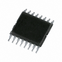
74LV4052PW,112 NXP Semiconductors, 74LV4052PW,112 Datasheet - Page 2

74LV4052PW,112
Manufacturer Part Number
74LV4052PW,112
Description
IC MUX/DEMUX DUAL 4X1 16TSSOP
Manufacturer
NXP Semiconductors
Series
74LVr
Type
Analog Multiplexerr
Datasheet
1.74LV4052DB118.pdf
(16 pages)
Specifications of 74LV4052PW,112
Function
Multiplexer/Demultiplexer
Circuit
2 x 4:1
On-state Resistance
60 Ohm
Voltage Supply Source
Single Supply
Voltage - Supply, Single/dual (±)
2.7 V ~ 3.6 V
Current - Supply
80µA
Operating Temperature
-40°C ~ 125°C
Mounting Type
Surface Mount
Package / Case
16-TSSOP (0.173", 4.40mm Width)
Multiplexer Configuration
Dual 4:1
Number Of Inputs
8
Number Of Outputs
2
Number Of Channels
2
Analog Switch On Resistance
250@1.2VOhm
Package Type
TSSOP
Power Supply Requirement
Single
Single Supply Voltage (min)
1V
Single Supply Voltage (typ)
3.3V
Single Supply Voltage (max)
6V
Dual Supply Voltage (min)
Not RequiredV
Dual Supply Voltage (typ)
Not RequiredV
Dual Supply Voltage (max)
Not RequiredV
Power Dissipation
400mW
Mounting
Surface Mount
Pin Count
16
Operating Temp Range
-40C to 125C
Operating Temperature Classification
Automotive
Lead Free Status / RoHS Status
Lead free / RoHS Compliant
Other names
74LV4052PW
74LV4052PW
935174950112
74LV4052PW
935174950112
1. C
2. The condition is V
Philips Semiconductors
FEATURES
QUICK REFERENCE DATA
GND = 0 V; T
NOTES:
ORDERING INFORMATION
PIN CONFIGURATION
t
t
C
C
C
16-Pin Plastic DIL
16-Pin Plastic SO
16-Pin Plastic SSOP Type II
16-Pin Plastic TSSOP Type I
1998 Jun 23
PZH
PHZ
SYMBOL
Optimized for low voltage applications: 1.0 to 6.0 V
Accepts TTL input levels between V
Low typ “ON” resistance:
60 W at V
90 W at V
145 W at V
Logic level translation: to enable 3 V logic to communicate with
V analog signals
Typical “break before make” built in
Analog/Digital multiplexing and demultiplexing
Signal gating
Output capability: non-standard
I
Dual 4-channel analog multiplexer/demultiplexer
I
PD
S
CC
P
f
f
V
i
o
PD
D
CC
= input frequency in MHz; C
/t
/t
= output frequency in MHz; C
((C
category: MSI
PZL
PLZ
= C
is used to determine the dynamic power dissipation (P
= supply voltage in V;
L
PD
+C
cc
cc
PACKAGES
cc
amb
S
– V
– V
Turn “ON” time
E or V
Turn “OFF” time
E or V
Input capacitance
Power dissipation capacitance per switch
Maximum switch capacitance
independent (Y) common (Z)
)
– V
V
CC
= 25 C; t
EE
EE
V
EE
CC
2
GND
= 4.5 V
= 3.0 V
OS
OS
2Y
2Y
2Y
2Y
V
I
= 2.0 V
2
2Z
EE
= GND to V
E
f
0
2
3
1
i
S
S
) ((C
n
n
f
1
2
3
4
8
5
6
7
o
r
) = sum of the outputs.
=t
PARAMETER
f
2.5 ns
L +
L
CC
= output load capacity in pF;
S
C
.
= maximum switch capacitance in pF;
S
CC
)
TEMPERATURE RANGE
SV01697
= 2.7 V and V
V
16
15
14
13
12
10
11
9
CC
–40 C to +125 C
–40 C to +125 C
–40 C to +125 C
–40 C to +125 C
V
1Y
1Y
1Z
1Y
1Y
S
S
2
CC
0
1
2
1
0
3
f
o
) where:
CC
= 3.6 V
C
R
V
V
See Notes 1 and 2
L
L
CC
= 15 pF
= 1KW
D
= 3.3 V
in W)
3
3 3 V
OUTSIDE NORTH AMERICA
2
DESCRIPTION
The 74LV4052 is a low-voltage CMOS device and is pin and
function compatible with the 74HC/HCT4052.
The 74LV4052 is a dual 4-channel analog multiplexer/demultiplexer
with a common select logic. Each multiplexer has four independent
inputs/outputs (nY
common channel select logics include two digital select inputs (S
and S
With E LOW, one of the four switches is selected (low impedance
ON-state) by S
impedance OFF-state, independent of S
the supply voltage pins for the digital control inputs (S
The V
(nY
V
operation as a digital multiplexer/demultiplexer, V
GND (typically ground).
PIN DESCRIPTION
74LV4052 PW
74LV4052 DB
PIN NUMBER
1, 5, 2, 4
6
7
8
10, 9
12, 14, 15, 11
13, 3
16
EE
CONDITIONS
74LV4052 N
74LV4052 D
0
, to nY
as a negative limit. V
1
CC
) and an active LOW enable input (E).
to GND ranges are 1.0 to 6.0 V. The analog inputs/outputs
3
, and nZ) can swing between V
0
and S
2Y
E
V
GND
S
1Y
1Z, 2Z
V
0
EE
0
CC
to nY
SYMBOL
, S
0
0
, 2Y
1.
to 1Y
1
With E HIGH, all switches are in the high
3
CC
3
) and a common input/output (nZ). The
NORTH AMERICA
74LV4052PW DH
3
- V
74LV4052 DB
74LV4052 N
74LV4052 D
EE
Independent inputs/outputs
Enable input (active LOW)
Negative supply voltage
Ground (0 V)
Select inputs
Independent inputs/outputs
Common inputs/outputs
Positive supply voltage
may not exceed 6.0 V. For
0
TYPICAL
and S
CC
30
22
57
12
FUNCTION
3.5
5
Product specification
as a positive limit and
74LV4052
1
. V
EE
853-1999 19618
CC
is connected to
SOT109-1
SOT338-1
SOT403-1
SOT38-4
0
, S
and GND are
Code
1
and E).
UNIT
ns
ns
pF
F
0


