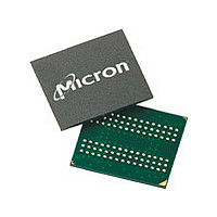
MT48LC4M32LFF5-10:G TR Micron Technology Inc, MT48LC4M32LFF5-10:G TR Datasheet - Page 65

MT48LC4M32LFF5-10:G TR
Manufacturer Part Number
MT48LC4M32LFF5-10:G TR
Description
Manufacturer
Micron Technology Inc
Type
Mobile SDRAMr
Datasheet
1.MT48LC4M32LFF5-10G_TR.pdf
(79 pages)
Specifications of MT48LC4M32LFF5-10:G TR
Organization
4Mx32
Density
128Mb
Address Bus
14b
Access Time (max)
22/8/7ns
Maximum Clock Rate
100MHz
Operating Supply Voltage (typ)
3.3V
Package Type
VFBGA
Operating Temp Range
0C to 70C
Operating Supply Voltage (max)
3.6V
Operating Supply Voltage (min)
3V
Supply Current
110mA
Pin Count
90
Mounting
Surface Mount
Operating Temperature Classification
Commercial
Lead Free Status / Rohs Status
Not Compliant
Figure 45:
PDF: 09005aef807f4885/Source: 09005aef8071a76b
128Mbx16x32Mobile_2.fm - Rev. L 10/07 EN
DQMU, DQML
A0–A9, A11
COMMAND
BA0, BA1
CLK
CKE
A10
DQ
t CMS
t CKS
t AS
t AS
t AS
Single Read – Without Auto Precharge
ACTIVE
ROW
ROW
T0
BANK
t CMH
t CKH
t AH
t AH
t AH
Notes:
t CK
t RCD
t RAS
t RC
T1
NOP
1. For this example, BL = 4, CL = 2, and the READ burst is followed by a “manual” PRECHARGE.
2. x16: A9 and A11 = “Don’t Care.”
3. PRECHARGE command not allowed or
x32: A8, A9, and A11 = “Don’t Care.”
See Table 17 on page 52.
DISABLE AUTO PRECHARGE
t CMS
t CL
COLUMN m
T2
BANK
READ
t CMH
t CH
CAS Latency
2
T3
NOP
t LZ
3
t AC
65
T4
D
NOP
OUT
t OH
t HZ
3
m
t
Micron Technology, Inc., reserves the right to change products or specifications without notice.
SINGLE BANKS
RAS would be violated.
PRECHARGE
ALL BANKS
BANK(S)
T5
t RP
128Mb: x16, x32 Mobile SDRAM
T6
NOP
©2001 Micron Technology, Inc. All rights reserved.
ACTIVE
ROW
BANK
ROW
T7
UNDEFINED
Timing Diagrams
T8
NOP
DON’T CARE


