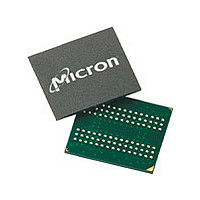
MT48LC4M32LFF5-10:G TR Micron Technology Inc, MT48LC4M32LFF5-10:G TR Datasheet - Page 7

MT48LC4M32LFF5-10:G TR
Manufacturer Part Number
MT48LC4M32LFF5-10:G TR
Description
Manufacturer
Micron Technology Inc
Type
Mobile SDRAMr
Datasheet
1.MT48LC4M32LFF5-10G_TR.pdf
(79 pages)
Specifications of MT48LC4M32LFF5-10:G TR
Organization
4Mx32
Density
128Mb
Address Bus
14b
Access Time (max)
22/8/7ns
Maximum Clock Rate
100MHz
Operating Supply Voltage (typ)
3.3V
Package Type
VFBGA
Operating Temp Range
0C to 70C
Operating Supply Voltage (max)
3.6V
Operating Supply Voltage (min)
3V
Supply Current
110mA
Pin Count
90
Mounting
Surface Mount
Operating Temperature Classification
Commercial
Lead Free Status / Rohs Status
Not Compliant
Figure 2:
PDF: 09005aef807f4885/Source: 09005aef8071a76b
128Mbx16x32Mobile_2.fm - Rev. L 10/07 EN
BA0, BA1
A0-A11,
CAS#
RAS#
WE#
CKE
CLK
CS#
14
ADDRESS
REGISTER
Functional Block Diagram 8 Meg x 16 SDRAM
MODE REGISTER
CONTROL
LOGIC
12
The 128Mb SDRAM device uses an internal pipelined architecture to achieve high-speed
operation. This architecture is compatible with the 2n rule of prefetch architectures, but
it also enables the column address to be changed on every clock cycle to achieve a high-
speed, fully random access. Precharging one bank while accessing one of the other three
banks will hide the precharge cycles and provide seamless high-speed, random-access
operation.
The 128Mb SDRAM device is designed to operate in 3.3V or 2.5V low-power memory
systems. The 2.5V version is compatible with 1.8V I/O interface. An auto refresh mode is
provided along with a power-saving, power-down mode. All inputs and outputs are
LVTTL-compatible.
SDRAMs offer substantial advances in DRAM operating performance, including the
ability to synchronously burst data at a high data rate with automatic column-address
generation, the ability to interleave between internal banks to hide precharge time, and
the capability to randomly change column addresses on each clock cycle during a burst
access.
COUNTER
REFRESH
12
9
2
12
ADDRESS
2
ROW-
MUX
COUNTER/
COLUMN-
CONTROL
ADDRESS
LATCH
BANK
LOGIC
12
DECODER
ADDRESS
BANK0
LATCH
ROW-
&
9
7
4096
READ DATA LATCH
SENSE AMPLIFIERS
DQM MASK LOGIC
(4,096 x 512 x 16)
WRITE DRIVERS
I/O GATING
DECODER
COLUMN
MEMORY
Micron Technology, Inc., reserves the right to change products or specifications without notice.
BANK0
ARRAY
4,096
(x16)
512
BANK1
BANK2
128Mb: x16, x32 Mobile SDRAM
BANK3
16
16
2
General Description
©2001 Micron Technology, Inc. All rights reserved.
REGISTER
REGISTER
OUTPUT
DATA
DATA
INPUT
2
16
DQML,
DQMH
DQ0-
DQ15


