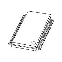
PCF8562TT NXP Semiconductors, PCF8562TT Datasheet - Page 17

PCF8562TT
Manufacturer Part Number
PCF8562TT
Description
Manufacturer
NXP Semiconductors
Datasheet
1.PCF8562TT.pdf
(36 pages)
Specifications of PCF8562TT
Operating Supply Voltage (typ)
2.5/3.3/5V
Number Of Digits
16
Number Of Segments
128
Operating Temperature (min)
-40C
Operating Temperature (max)
85C
Operating Temperature Classification
Industrial
Package Type
TSSOP
Pin Count
48
Mounting
Surface Mount
Power Dissipation
400mW
Frequency (max)
400KHz
Operating Supply Voltage (min)
1.8V
Operating Supply Voltage (max)
5.5V
Lead Free Status / Rohs Status
Compliant
Available stocks
Company
Part Number
Manufacturer
Quantity
Price
Part Number:
PCF8562TT
Manufacturer:
NXP/恩智浦
Quantity:
20 000
Company:
Part Number:
PCF8562TT/2
Manufacturer:
NXP Semiconductors
Quantity:
36 137
Company:
Part Number:
PCF8562TT/2
Manufacturer:
NXP
Quantity:
12 000
Part Number:
PCF8562TT/2
Manufacturer:
NXP/恩智浦
Quantity:
20 000
Company:
Part Number:
PCF8562TT/2Ј¬118
Manufacturer:
NXP
Quantity:
64 000
NXP Semiconductors
PCF8562_2
Product data sheet
6.12 Device select
6.13 Output bank selector
6.14 Input bank selector
The addressing mechanism for the display RAM is realized using the data pointer. This
allows the loading of an individual display data byte, or a series of display data bytes, into
any location of the display RAM. The sequence commences with the initialization of the
data pointer by the Load Data Pointer command. Following this, an arriving data byte is
stored at the display RAM address indicated by the data pointer in accordance with the
filling order shown in
are automatically incremented by a value dependent on the selected LCD drive mode:
eight (static drive mode), four (1 : 2 mode), three (1 : 3 mode) or two (1 : 4 mode). If an
I
The data pointer should be re-written prior to further RAM access.
Storage is allowed to take place when the internal select register agrees with the
hardware subaddress applied to A0, A1 and A2.
The hardware subaddress should not be changed whilst the device is being accessed on
the I
The output bank selector selects one of the four bits per display RAM address for transfer
to the display latch. The actual bit chosen depends on the selected LCD drive mode and
on the instant in the multiplex sequence. In 1 : 4 mode, all RAM addresses of bit 0 are
selected, these are followed by the contents of bit 1, bit 2 and then bit 3. Similarly in 1 : 3
mode, bits 0, 1 and 2 are selected sequentially. In 1 : 2 mode, bits 0 and 1 are selected
and, in static mode, bit 0 is selected. Signal SYNC will reset these sequences to the
following starting points; bit 3 for 1 : 4 mode, bit 2 for 1 : 3 mode, bit 1 for 1 : 2 mode and
bit 0 for static mode.
The PCF8562 includes a RAM bank switching feature in the static and 1 : 2 drive modes.
In the static drive mode, the Bank Select command may request the contents of bit 2 to be
selected for display instead of the contents of bit 0. In 1 : 2 mode, the contents of
bits 2 and 3 may be selected instead of bits 0 and 1. This allows display information to be
prepared in an alternative bank and then selected for display when it is assembled.
The input bank selector loads display data into the display RAM in accordance with the
selected LCD drive configuration. The Bank Select command can be used to load display
data in bit 2 in static drive mode or in bits 2 and 3 in 1 : 2 mode. The input bank selector
functions are independent of the output bank selector.
2
C-bus data access is terminated early then the state of the data pointer will be unknown.
2
C-bus interface.
Figure
Rev. 02 — 22 January 2007
10. After each byte is stored, the contents of the data pointer
Universal LCD driver for low multiplex rates
PCF8562
© NXP B.V. 2007. All rights reserved.
17 of 36


