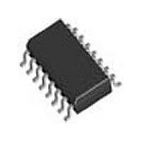
TC74HC123AFN Toshiba, TC74HC123AFN Datasheet - Page 5

TC74HC123AFN
Manufacturer Part Number
TC74HC123AFN
Description
Manufacturer
Toshiba
Datasheet
1.TC74HC123AFN.pdf
(14 pages)
Specifications of TC74HC123AFN
Logic Family
HC
High Level Output Current
-5.2mA
Low Level Output Current
5.2mA
Quiescent Current
4uA
Number Of Elements
2
Operating Temperature Classification
Industrial
Operating Supply Voltage (max)
6V
Operating Supply Voltage (typ)
2.5/3.3/5V
Operating Temperature (min)
-40C
Operating Temperature (max)
85C
Technology
CMOS
Abs. Propagation Delay Time
295ns
Operating Supply Voltage (min)
2V
Lead Free Status / Rohs Status
Not Compliant
Functional Description
(1)
(2)
(3)
(4)
Stand-by state
triggering, the Q
comparators that relate to the timing of the output pulse, and two reference voltage supplies turn off.
The total supply current is only leakage current.
Trigger operation
input is low, and the B input has a rising signal; second, where the B input is high, and the A input
has a falling signal; and third, where the A input is low and the B input is high, and the CLR
input has a rising signal.
external capacitor discharges through Q
voltage level falls to the internal reference voltage Vref L, the output of C1 becomes low. The flip-flop
is then reset and Q
constant of external capacitor Cx and resistor Rx.
stays high even if the voltage of Rx/Cx changes from falling to rising. When Rx/Cx reaches the
internal reference voltage Vref H, the output of C2 becomes low, the output Q goes low and C2 stops
its operation. That means, after triggering, when the voltage level of the Rx/Cx node reaches Vref H,
the IC returns to its MONOSTABLE state.
delays of the IC, the width of the output pulse, tw (OUT), is as follows:
Retrigger operation
effective only if the IC is charging Cx. The voltage level of the Rx/Cx node then falls to Vref L level
again. Therefore the Q output stays high if the next trigger comes in before the time period set by Cx
and Rx.
it will have no effect.
Reset operation
the Q output is held low and the trigger control F/F is reset. Also, Q
rapidly to V
The external capacitor (Cx) is fully charged to V
Trigger operation is effective in any of the following three cases. First, the condition where the A
After a trigger becomes effective, comparators C1 and C2 start operating, and Q
After Q
Upon triggering, output Q becomes high, following some delay time of the internal F/F and gates. It
With large values of Cx and Rx, and ignoring the discharge time of the capacitor and internal
When a new trigger is applied to either input A or B while in the MONOSTABLE state, it is
If the new trigger is very close to previous trigger, such as an occurrence during the discharge cycle,
The minimum time for a trigger to be effective 2nd trigger, trr (Min.), depends on V
In normal operation, the CLR input is held high. If CLR is low, a trigger has no effect because
This means if CLR is set low, the IC goes into a wait state.
tw (OUT) = 1.0 Cx Rx
N
turns off, the voltage at the Rx/Cx node starts rising at a rate determined by the time
CC
.
P
and Q
N
turns off. At that moment C1 stops but C2 continues operating.
N
transistors which are connected to the Rx/Cx node are in the off state. Two
N
. The voltage level at the Rx/Cx node drops. If the Rx/Cx
5
CC
in the stand-by state. That means, before
TC74HC123AP/AF/AFN
P
turns on and Cx is charged
N
is turned on. The
CC
2007-10-01
and Cx.


