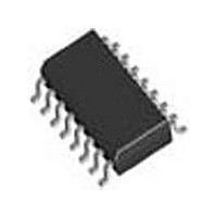
TC74HC123AFN Toshiba, TC74HC123AFN Datasheet - Page 6

TC74HC123AFN
Manufacturer Part Number
TC74HC123AFN
Description
Manufacturer
Toshiba
Datasheet
1.TC74HC123AFN.pdf
(14 pages)
Specifications of TC74HC123AFN
Logic Family
HC
High Level Output Current
-5.2mA
Low Level Output Current
5.2mA
Quiescent Current
4uA
Number Of Elements
2
Operating Temperature Classification
Industrial
Operating Supply Voltage (max)
6V
Operating Supply Voltage (typ)
2.5/3.3/5V
Operating Temperature (min)
-40C
Operating Temperature (max)
85C
Technology
CMOS
Abs. Propagation Delay Time
295ns
Operating Supply Voltage (min)
2V
Lead Free Status / Rohs Status
Not Compliant
Absolute Maximum Ratings (Note 1)
Operating Ranges (Note 1)
Supply voltage range
DC input voltage
DC output voltage
Input diode current
Output diode current
DC output current
DC V
Power dissipation
Storage temperature
Note 1: Exceeding any of the absolute maximum ratings, even briefly, lead to deterioration in IC performance or
Note 2: 500 mW in the range of Ta = −40 to 65°C. From Ta = 65 to 85°C a derating factor of −10 mW/°C shall be
Supply voltage
Input voltage
Output voltage
Operating temperature
Input rise and fall time
( CLR only)
External capacitor
External resistor
Note 1: The operating ranges must be maintained to ensure the normal operation of the device.
Note 2: The maximum allowable values of Cx and Rx are a function of leakage of capacitor Cx, the leakage of
CC
/ground current
even destruction.
Using continuously under heavy loads (e.g. the application of high temperature/current/voltage and the
significant change in temperature, etc.) may cause this product to decrease in the reliability significantly
even if the operating conditions (i.e. operating temperature/current/voltage, etc.) are within the absolute
maximum ratings and the operating ranges.
Please design the appropriate reliability upon reviewing the Toshiba Semiconductor Reliability Handbook
(“Handling Precautions”/“Derating Concept and Methods”) and individual reliability data (i.e. reliability test
report and estimated failure rate, etc).
applied until 300 mW.
Unused inputs must be tied to either VCC or GND.
TC74HC123A, and leakage due to board layout and surface resistance.
Susceptibility to externally induced noise signals may occur for Rx > 1 MΩ.
Characteristics
Characteristics
Symbol
Symbol
V
V
I
V
V
T
T
OUT
t
V
I
I
V
P
OUT
OUT
Cx
Rx
I
r
OK
CC
CC
stg
CC
opr
IK
, t
IN
IN
D
f
500 (DIP) (Note 2)/180 (SOP)
0 to 1000 (V
6
0 to 500 (V
0 to 400 (V
≥ 5 k (V
≥ 1 k (V
− 0.5 to V
− 0.5 to V
No limitation
− 65 to 150
− 40 to 85
− 0.5 to 7
0 to V
0 to V
Rating
Rating
2 to 6
CC
CC
± 20
± 20
± 25
± 50
CC
CC
CC
CC
CC
= 2.0 V) (Note 2)
≥ 3.0 V) (Note 2)
CC
CC
= 4.5 V)
= 6.0 V)
+ 0.5
+ 0.5
= 2.0 V)
(Note 2)
TC74HC123AP/AF/AFN
Unit
mW
Unit
mA
mA
mA
mA
°C
°C
ns
V
V
V
V
V
V
Ω
F
2007-10-01


