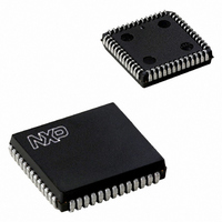
SC28C94A1A,518 NXP Semiconductors, SC28C94A1A,518 Datasheet - Page 27

SC28C94A1A,518
Manufacturer Part Number
SC28C94A1A,518
Description
IC UART QUAD W/FIFO 52-PLCC
Manufacturer
NXP Semiconductors
Datasheet
1.SC28C94A1A518.pdf
(39 pages)
Specifications of SC28C94A1A,518
Features
False-start Bit Detection
Number Of Channels
4, QUART
Fifo's
8 Byte
Voltage - Supply
5V
With Auto Flow Control
Yes
With False Start Bit Detection
Yes
With Modem Control
Yes
With Cmos
Yes
Mounting Type
Surface Mount
Package / Case
52-PLCC
Lead Free Status / RoHS Status
Lead free / RoHS Compliant
Other names
568-1114-2
935262534518
SC28C94A1A-T
935262534518
SC28C94A1A-T
Available stocks
Company
Part Number
Manufacturer
Quantity
Price
Company:
Part Number:
SC28C94A1A,518
Manufacturer:
Maxim
Quantity:
21
Company:
Part Number:
SC28C94A1A,518
Manufacturer:
NXP Semiconductors
Quantity:
10 000
1. The minimum time indicates that read data will remain valid until the bus master drives CEN and/or RDN to High.
2. The fact that this parameter is negative means that the Dnn line may actually become valid after CEN and WRN are both Low.
3. In a Write operation, the bus master must hold the write data valid either until drives CEN and/or WRN to High, or until the QUART drives
4. Test condition for interrupt and I/O outputs: C
Philips Semiconductors
AC ELECTRICAL CHARACTERISTICS
V
NOTES:
5. Consecutive write operations to the upper four bits of the Command Register (CR) require at least three X1/CLK edges; four X1/CLK edges
6. Address is latched at leading edge of a read or write cycle.
2006 Aug 09
CC
Quad universal asynchronous receiver/transmitter (QUART)
NO
NO.
DACKN to Low, whichever comes first.
V
in the ‘X1/CLK divide by 2 edges’ according to register 2Eh or 2Fh setting.
10
1
2
3
4
5
6
7
8
9
= 5V
CC
DACKN
X1/CLK
. Test condition for rest of outputs: C
A[5:0]
D[7:0]
WRN
CEN
RDN
FIGURE
FIGURE
10%, T
5
5
5
5
5
5
5
5
5
5
A
= –40 C to +85 C, unless otherwise specified.
Setup: A[5:0] valid to CEN Low
Hold: A[5:0] valid after CEN Low
Access: Later of CEN Low and RDN Low, to Dnn valid (read)
Later of CEN Low and (RDN or WRN as applicable) Low, to DACKN Low
Earlier of CEN High or RDN High, to Dnn released (read)
Earlier of CEN High or (RDN or WRN as applicable) High, to DACKN released
Earlier of CEN High or (RDN or WRN as applicable) High, in one cycle, to later
of CEN Low and (RDN or WRN as applicable) Low, for the next cycle
Setup, Dnn valid (write) to later of CEN Low and WRN Low
Later of CEN Low and WRN Low, to earlier of CEN High or WRN High
Hold: Dnn valid (write) after DACKN Low, CEN High or WRN High
Normal Operation:
From Power Down:
1
2
3
Figure 5. A Read Cycle Followed by a Write Cycle with DACKN
4
3
4
L
= 150 pF
L
CHARACTERISTIC
CHARACTERISTIC
4
= 50 pF, forced current for V
READ CYCLE
6
5
6
5
6
27
7
7
7
7
OL
1
2
= 4.0 mA; forced current for V
1
8
8
3
2
4
4
9
X1 edges
WRITE CYCLE
110/115
9
10 + 2
9
Min
–30
9
10
45
50
0
0
0
5
OH
LIMITS
Typ
= 400 A, RL = 2.7 k to
10
10
6
10
90/122 + 3
X1 edges
6
110/115
SC28C94
Max
Product data sheet
150
30
30
SD00677
5
UNIT
UNIT
ns
ns
ns
ns
ns
ns
ns
ns
ns
ns


