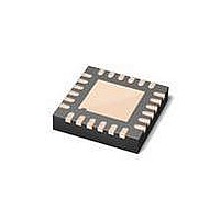
MAX3107ETG+ Maxim Integrated Products, MAX3107ETG+ Datasheet - Page 15

MAX3107ETG+
Manufacturer Part Number
MAX3107ETG+
Description
IC UART SPI/I2C 128 FIFO 24TQFN
Manufacturer
Maxim Integrated Products
Datasheet
1.MAX3107EAG.pdf
(52 pages)
Specifications of MAX3107ETG+
Features
Internal Oscillators
Number Of Channels
4, QUART
Fifo's
128 Byte
Protocol
RS232, RS485
Voltage - Supply
2.35 V ~ 3.6 V
With Auto Flow Control
Yes
With Irda Encoder/decoder
Yes
With False Start Bit Detection
Yes
Mounting Type
Surface Mount
Package / Case
24-TQFN Exposed Pad
Data Rate
24 Mbps
Supply Voltage (max)
3.3 V
Supply Voltage (min)
2.35 V
Supply Current
0.64 mA
Maximum Operating Temperature
+ 85 C
Minimum Operating Temperature
- 40 C
Mounting Style
SMD/SMT
No. Of Channels
1
Uart Features
128-Word Transmit / Receive FIFO, Half-Duplex Echo Suppression, Shutdown And Autosleep Modes
Supply Voltage Range
2.35V To 3.6V
Rohs Compliant
Yes
Lead Free Status / RoHS Status
Lead free / RoHS Compliant
The MAX3107 UART is a bridge between an SPI/
MICROWIRE™ or I
asynchronous serial-data communication link, such as
RS-485, RS-232, or IrDA. The MAX3107 contains an
advanced UART, a fractional baud-rate generator, and
four GPIOs. The MAX3107 is configured and monitored,
and data is written and read from 8-bit registers through
SPI or I
function as shown in the Register Map.
The host controller loads and transmits data into the
Transmit Holding register (THR) through SPI or I
data is automatically pushed into the transmit FIFO and
sent out at TX. The MAX3107 adds START, STOP, and
parity bits to the data and sends the data out at the
selected baud rate. The clock configuration registers
determine the baud rate, clock source selection, and
clock frequency prescaling.
The receiver in the MAX3107 detects a START bit as a
high-to-low RX transition. An internal clock samples this
data. The received data is automatically placed in the
receive FIFO and can then be read out of the RxFIFO
through the RHR.
The MAX3107 has a flat register structure without shad-
ow registers. The registers are 8 bits wide. The MAX3107
registers have some similarities to the 16C550 registers.
The UART’s receiver and the transmitter each have a
128-word deep FIFO, reducing the intervals that the host
processor needs to dedicate for high-speed, high-vol-
ume data transfer. As the data rates of the asynchronous
RX, TX interfaces increase and get closer to those of the
host controller’s SPI/I
and flow control can make up a significant portion of the
host’s activity. By increasing FIFO size, the host is inter-
rupted less often and can utilize SPI/I
transfers to/from the FIFOs.
FIFO trigger levels can generate interrupts to the host
controller, signaling that programmed FIFO fill levels
have been reached. The transmitter and receiver trig-
ger levels are programmed through FIFOTrgLvl with a
resolution of eight FIFO locations. When a receive FIFO
trigger is generated, the host knows that the receive
FIFO has a defined number of words waiting to be read
out or that a known number of vacant FIFO locations are
MICROWIRE is a trademark of National Semiconductor Corp.
2
C. These registers are organized by related
______________________________________________________________________________________
Receive and Transmit FIFOs
2
2
C microprocessor bus and an
C data rates, UART management
Detailed Description
SPI/I
2
C burst data block
Register Set
2
C UART with 128-Word FIFOs
2
C. This
available and ready to be filled. The transmit FIFO trig-
ger generates an interrupt when the transmit FIFO level
is above the programmed trigger level. The host then
knows to throttle data writing to the transmit FIFO.
The host can read out the number of words present in each
of the FIFOs through the TxFIFOLvl and RxFIFOLvl registers.
Figure 3 shows the structure of the transmitter with the
TxFIFO. The transmit FIFO can hold up to 128 words that
are written to it through THR.
The current number of words in the TxFIFO can be read
out through the TxFIFOLvl register. The transmit FIFO
can be programmed to generate an interrupt when a
programmed number of words are present in the TxFIFO
through the FIFOTrgLvl register. The TxFIFO interrupt
trigger level is selectable through FIFOTrgLvl[3:0]. When
the transmit FIFO fill level reaches the programmed trig-
ger level, the ISR[4] interrupt is set.
The transmit FIFO is empty when ISR[5]: TxEmtyInt is set.
ISR[5] turns high when the transmitter starts transmit-
ting the last word in the TxFIFO. Hence, the transmitter
is completely empty after ISR[5] is set with an addi-
tional delay equal to the length of a complete character
(including START, parity, and STOP bits).
The contents of the TxFIFO and RxFIFOs are both
cleared through MODE2[1]: FIFORst.
Figure 3. Transmit FIFO Signals
and Internal Oscillator
TxFIFOLvl
ISR[4]
ISR[5]
DATA FROM SPI/I
TRIGGER
EMPTY
LEVEL
2
C INTERFACE
CURRENT FILL LEVEL
Transmitter Operation
TRANSMIT FIFO
FIFOTrgLvl[3:0]
TRANSMITTER
THR
128
3
2
1
TX
15


