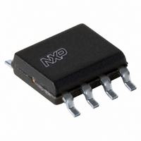
TDA8541T/N1,112 NXP Semiconductors, TDA8541T/N1,112 Datasheet - Page 3

TDA8541T/N1,112
Manufacturer Part Number
TDA8541T/N1,112
Description
IC AMP AUDIO PWR 1.2W MONO 8SOIC
Manufacturer
NXP Semiconductors
Type
Class ABr
Datasheet
1.TDA8541TN1118.pdf
(18 pages)
Specifications of TDA8541T/N1,112
Output Type
1-Channel (Mono)
Package / Case
8-SOIC (3.9mm Width)
Max Output Power X Channels @ Load
1.2W x 1 @ 8 Ohm
Voltage - Supply
2.2 V ~ 18 V
Features
Depop, Mute, Short-Circuit and Thermal Protection, Standby
Mounting Type
Surface Mount
Product
Class-AB
Output Power
1.2 W
Available Set Gain
30 dB
Thd Plus Noise
0.15 %
Operating Supply Voltage
5 V
Supply Current
8 mA
Maximum Power Dissipation
800 mW
Maximum Operating Temperature
+ 85 C
Mounting Style
SMD/SMT
Audio Load Resistance
8 Ohms
Input Bias Current (max)
500 nA
Input Signal Type
Differential or Single
Minimum Operating Temperature
- 40 C
Output Signal Type
Differential, Single
Supply Type
Single
Supply Voltage (max)
18 V
Supply Voltage (min)
2.2 V
Lead Free Status / RoHS Status
Lead free / RoHS Compliant
Other names
568-3475-5
935211650112
TDA8541TD
935211650112
TDA8541TD
NXP Semiconductors
BLOCK DIAGRAM
FUNCTIONAL DESCRIPTION
The TDA8541(T) is a BTL audio power amplifier capable
of delivering 1 W output power to an 8 Ω load at
THD = 10% using a 5 V power supply. Using the MODE
pin the device can be switched to standby and mute
condition. The device is protected by an internal thermal
shutdown protection mechanism. The gain can be set
within a range from 6 dB to 30 dB by external feedback
resistors.
Power amplifier
The power amplifier is a Bridge Tied Load (BTL) amplifier
with a complementary PNP-NPN output stage.
The voltage loss on the positive supply line is the
saturation voltage of a PNP power transistor, on the
negative side the saturation voltage of an NPN power
transistor. The total voltage loss is <1 V and with a 5 V
supply voltage and an 8 Ω loudspeaker an output power of
1 W can be delivered.
1998 Apr 01
handbook, halfpage
1 W BTL audio amplifier
MODE
V CC
SVR
IN−
IN+
4
3
6
2
1
−
+
−
20 kΩ
20 kΩ
Fig.1 Block diagram.
STANDBY/MUTE LOGIC
R
TDA8541
−
−
+
R
GND
7
5
8
MGB972
OUT−
OUT+
3
PINNING
Mode select pin
The device is in standby mode (with a very low current
consumption) if the voltage at the MODE pin is
>(V
level of less than 0.5 V the amplifier is fully operational.
In the range between 1.5 V and V
is in mute condition. The mute condition is useful to
suppress plop noise at the output, caused by charging of
the input capacitor.
handbook, halfpage
MODE
SVR
IN+
IN−
OUT−
V
GND
OUT+
CC
SYMBOL
CC
− 0.5 V), or if this pin is floating. At a MODE voltage
MODE
SVR
IN+
IN−
Fig.2 Pin configuration.
PIN
1
2
3
4
5
6
7
8
1
2
3
4
operating mode select (standby,
mute, operating)
ripple rejection
positive input
negative input
negative loudspeaker terminal
supply voltage
ground
positive loudspeaker terminal
TDA8541
half supply voltage, decoupling
MGB971
DESCRIPTION
CC
7
6
5
8
− 1.5 V the amplifier
Product specification
OUT+
V CC
OUT−
GND
TDA8541


